- 您现在的位置:买卖IC网 > PDF目录11486 > ADV3220ACPZ (Analog Devices Inc)IC MULTIPLEXER 2:1 16LFCSP PDF资料下载
参数资料
| 型号: | ADV3220ACPZ |
| 厂商: | Analog Devices Inc |
| 文件页数: | 16/20页 |
| 文件大小: | 0K |
| 描述: | IC MULTIPLEXER 2:1 16LFCSP |
| 标准包装: | 1 |
| 功能: | 多路复用器 |
| 电路: | 1 x 2:1 |
| 电压电源: | 双电源 |
| 电压 - 电源,单路/双路(±): | ±5V |
| 电流 - 电源: | 7.5mA |
| 工作温度: | -40°C ~ 85°C |
| 安装类型: | 表面贴装 |
| 封装/外壳: | 8-WFDFN 裸露焊盘,CSP |
| 供应商设备封装: | 8-LFCSP-WD(3x3) |
| 包装: | 托盘 |
ADV3219/ADV3220
Rev. 0 | Page 5 of 20
ABSOLUTE MAXIMUM RATINGS
POWER DISSIPATION
Table 3.
Parameter
Rating
Supply Voltage (V+ V)
12 V
Analog Input Voltage
V to V+
Digital Input Voltage
0 to V+
Output Voltage (Disabled Output)
(V+ 1 V) to (V + 1 V)
Output Short-Circuit
Duration
Momentary
Current
50 mA
Temperature
Storage Temperature Range
65°C to +150°C
Operating Temperature Range
40°C to +85°C
Junction Temperature
150°C
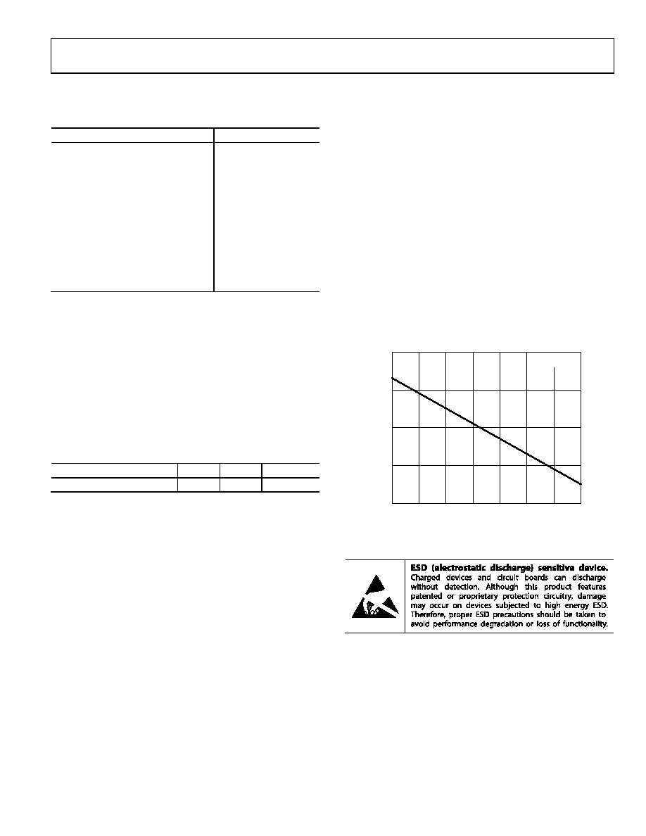
The ADV3219/ADV3220 are operated with ±5 V supplies and
can drive loads down to 150 Ω, resulting in a wide range of
possible power dissipations. For this reason, extra care must
be taken derating the operating conditions based on ambient
temperature.
Packaged in an 8-lead LFCSP, the ADV3219 and ADV3220
junction-to-ambient thermal impedance (θJA) is 85°C/W. For long-
term reliability, the maximum allowed junction temperature of the
die, TJ, should not exceed 125°C. Temporarily exceeding this
limit can cause a shift in parametric performance due to a change
in stresses exerted on the die by the package. Figure 2 shows the
range of the allowed internal die power dissipations that meet
these conditions over the 40°C to +85°C ambient temperature
range. When using Figure 2, do not include the external load
power in the maximum power calculation, but do include the
load current through the die output transistors.
Stresses above those listed under Absolute Maximum Ratings
may cause permanent damage to the device. This is a stress
rating only; functional operation of the device at these or any
other conditions above those indicated in the operational
section of this specification is not implied. Exposure to absolute
maximum rating conditions for extended periods may affect
device reliability.
1.5
0.3
0.6
0.9
1.2
15
25
35
45
55
65
75
85
MA
XI
MU
M
P
O
W
E
R
(W
)
AMBIENT TEMPERATURE (°C)
TJ = 125°C
08
64
9-
0
02
THERMAL RESISTANCE
θJA is specified for the worst-case conditions, that is, a device
soldered in a circuit board for surface-mount packages.
Table 4. Thermal Resistance
Package Type
θJA
θJC
Unit
8-Lead LFCSP
85
23
°C/W
Figure 2. Maximum Die Power Dissipation vs. Ambient Temperature
ESD CAUTION
相关PDF资料 |
PDF描述 |
|---|---|
| GRM319F51E105ZA01D | CAP CER 1UF 25V Y5V 1206 |
| ADV3219ACPZ | IC MULTIPLEXER 2:1 16LFCSP |
| GRM2197U2A4R7CD01D | CAP CER 4.7PF 100V U2J 0805 |
| ADG636YRUZ | IC SWITCH DUAL SPDT 14TSSOP |
| GRM2197U2A4R3CD01D | CAP CER 4.3PF 100V U2J 0805 |
相关代理商/技术参数 |
参数描述 |
|---|---|
| ADV3220ACPZ-R7 | 功能描述:IC MULTIPLEXER 2:1 16LFCSP RoHS:是 类别:集成电路 (IC) >> 接口 - 模拟开关,多路复用器,多路分解器 系列:- 标准包装:1,000 系列:- 功能:多路复用器 电路:1 x 4:1 导通状态电阻:- 电压电源:双电源 电压 - 电源,单路/双路(±):±5V 电流 - 电源:7mA 工作温度:-40°C ~ 85°C 安装类型:表面贴装 封装/外壳:16-SOIC(0.154",3.90mm 宽) 供应商设备封装:16-SOIC 包装:带卷 (TR) |
| ADV3220ACPZ-RL | 功能描述:IC MULTIPLEXER 2:1 16LFCSP RoHS:是 类别:集成电路 (IC) >> 接口 - 模拟开关,多路复用器,多路分解器 系列:- 标准包装:1,000 系列:- 功能:多路复用器 电路:1 x 4:1 导通状态电阻:- 电压电源:双电源 电压 - 电源,单路/双路(±):±5V 电流 - 电源:7mA 工作温度:-40°C ~ 85°C 安装类型:表面贴装 封装/外壳:16-SOIC(0.154",3.90mm 宽) 供应商设备封装:16-SOIC 包装:带卷 (TR) |
| ADV3220-EVALZ | 制造商:AD 制造商全称:Analog Devices 功能描述:800 MHz, 2:1 Analog Multiplexers |
| ADV3221 | 制造商:AD 制造商全称:Analog Devices 功能描述:800 MHz, 4:1 Analog Multiplexer |
| ADV3221ARZ | 功能描述:IC MULTIPLEXER 4:1 16SOIC RoHS:是 类别:集成电路 (IC) >> 接口 - 模拟开关,多路复用器,多路分解器 系列:- 应用说明:Ultrasound Imaging Systems Application Note 产品培训模块:Lead (SnPb) Finish for COTS Obsolescence Mitigation Program 标准包装:250 系列:- 功能:开关 电路:单刀单掷 导通状态电阻:48 欧姆 电压电源:单电源 电压 - 电源,单路/双路(±):2.7 V ~ 5.5 V 电流 - 电源:5µA 工作温度:0°C ~ 70°C 安装类型:表面贴装 封装/外壳:48-LQFP 供应商设备封装:48-LQFP(7x7) 包装:托盘 |
发布紧急采购,3分钟左右您将得到回复。