- 您现在的位置:买卖IC网 > PDF目录1901 > ADV7125WBCPZ170 (Analog Devices Inc)IC DAC VIDEO 3-CH 330MHZ 48VFQFN PDF资料下载
参数资料
| 型号: | ADV7125WBCPZ170 |
| 厂商: | Analog Devices Inc |
| 文件页数: | 15/16页 |
| 文件大小: | 0K |
| 描述: | IC DAC VIDEO 3-CH 330MHZ 48VFQFN |
| 标准包装: | 1 |
| 位数: | 8 |
| 转换器数目: | 3 |
| 电压电源: | 单电源 |
| 功率耗散(最大): | 30mW |
| 工作温度: | -40°C ~ 85°C |
| 安装类型: | 表面贴装 |
| 封装/外壳: | 48-VFQFN 裸露焊盘,CSP |
| 供应商设备封装: | 48-LFCSP-VQ(7x7) |
| 包装: | 托盘 |
| 输出数目和类型: | 6 电流,单极 |
| 采样率(每秒): | 170M |
ADV7125
Rev. C | Page 8 of 16
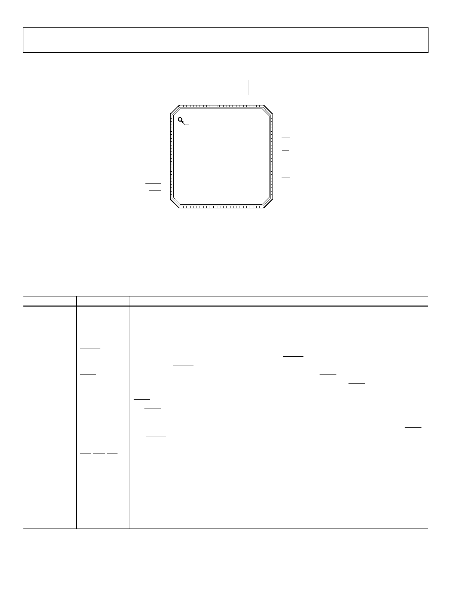
PIN CONFIGURATION AND FUNCTION DESCRIPTIONS
13
14
15
16
17
18
19
20
21
22
23
24
V
AA
GN
D
GN
D
B0
B1
B2
B3
B4
B5
B6
B7
CL
O
C
K
48
47
46
45
44
43
42
41
40
39
38
37
R7
R6
R5
R4
R3
R2
R1
R0
GN
D
GN
D
PS
A
VE
R
SE
T
1
2
3
4
5
6
7
8
9
10
11
12
GND
G0
G1
G2
G3
G4
G5
G6
G7
BLANK
SYNC
NOTES
1. THE LFCSP_VQ HAS AN EXPOSED PADDLE THAT MUST BE
CONNECTED TO GND.
COMP
VAA
IOB
GND
35
VREF
36
34
33
32
31
30
29
28
27
26
25
TOP VIEW
(Not to Scale)
ADV7125
PIN 1
INDICATOR
03
09
7-
00
3
IOG
IOR
Figure 3. Pin Configuration
Table 6. Pin Function Descriptions
Pin Number
Mnemonic
Description
1, 2, 14, 15, 25,
26, 39, 40
GND
Ground. All GND pins must be connected.
3 to 10, 16 to
23, 41 to 48
G0 to G7,
B0 to B7,
R0 to R7
Red, Green, and Blue Pixel Data Inputs (TTL Compatible). Pixel data is latched on the rising edge of
CLOCK. R0, G0, and B0 are the least significant data bits. Unused pixel data inputs should be
connected to either the regular printed circuit board (PCB) power or ground plane.
11
BLANK
Composite Blank Control Input (TTL Compatible). A Logic 0 on this control input drives the analog
outputs, IOR, IOB, and IOG, to the blanking level. The BLANK signal is latched on the rising edge of
CLOCK. While BLANK is a Logic 0, the R0 to R7, G0 to G7, and B0 to B7 pixel inputs are ignored.
12
SYNC
Composite Sync Control Input (TTL Compatible). A Logic 0 on the SYNC input switches off a
40 IRE current source. This is internally connected to the IOG analog output. SYNC does not override
any other control or data input; therefore, it should only be asserted during the blanking interval.
SYNC is latched on the rising edge of CLOCK. If sync information is not required on the green channel,
the SYNC input should be tied to Logic 0.
13, 29, 30
VAA
Analog Power Supply (5 V ± 5%). All VAA pins on the ADV7125 must be connected.
24
CLOCK
Clock Input (TTL Compatible). The rising edge of CLOCK latches the R0 to R7, G0 to G7, B0 to B7, SYNC,
and BLANK pixel and control inputs. It is typically the pixel clock rate of the video system. CLOCK
should be driven by a dedicated TTL buffer.
33, 31, 27
IOR, IOG, IOB
Differential Red, Green, and Blue Current Outputs (High Impedance Current Sources). These RGB video
outputs are specified to directly drive RS-343A and RS-170 video levels into a doubly terminated 75 Ω
load. If the complementary outputs are not required, these outputs should be tied to ground.
34, 32, 28
IOR, IOG, IOB
Red, Green, and Blue Current Outputs. These high impedance current sources are capable of directly
driving a doubly terminated 75 Ω coaxial cable. All three current outputs should have similar output
loads whether or not they are all being used.
35
COMP
Compensation Pin. This is a compensation pin for the internal reference amplifier. A 0.1 μF ceramic
capacitor must be connected between COMP and VAA.
36
VREF
Voltage Reference Input for DACs or Voltage Reference Output (1.235 V).
相关PDF资料 |
PDF描述 |
|---|---|
| ADV7171KSZ-REEL | IC DAC VIDEO ENC NTSC 44-MQFP |
| ADV7172KSTZ-REEL | IC DAC VIDEO NTSC 6-CH 48-LQFP |
| ADV7177KSZ-REEL | IC DAC VIDEO NTSC 3-CH 44MQFP |
| ADV7179KCPZ-REEL | IC ENCODER VID NTSC/PAL 40LFCSP |
| ADV7181CBSTZ | IC VIDEO DECODER SDTV RGB 64LQFP |
相关代理商/技术参数 |
参数描述 |
|---|---|
| ADV7125WBCPZ170-RL | 制造商:Rochester Electronics LLC 功能描述: 制造商:Analog Devices 功能描述: |
| ADV7125WBSTZ170 | 制造商:Analog Devices 功能描述:330MHZ TRIPLE 8-BIT HIGH SPEED VIDEO DAC - Rail/Tube |
| ADV7125WBSTZ170-RL | 制造商:AD 制造商全称:Analog Devices 功能描述:CMOS, 330 MHz Triple 8-Bit High Speed Video DAC |
| ADV7127 | 制造商:AD 制造商全称:Analog Devices 功能描述:CMOS, 240 MHz 10-Bit High Speed Video DAC |
| ADV7127JR240 | 制造商:Rochester Electronics LLC 功能描述:SINGLE HIGH SPEED VIDEO DAC I.C. - Bulk 制造商:Analog Devices 功能描述: |
发布紧急采购,3分钟左右您将得到回复。