- 您现在的位置:买卖IC网 > PDF目录8893 > ADV7127JRUZ240 (Analog Devices Inc)IC DAC VIDEO240MHZ 3.3/5 24TSSOP PDF资料下载
参数资料
| 型号: | ADV7127JRUZ240 |
| 厂商: | Analog Devices Inc |
| 文件页数: | 5/16页 |
| 文件大小: | 0K |
| 描述: | IC DAC VIDEO240MHZ 3.3/5 24TSSOP |
| 产品培训模块: | Data Converter Fundamentals DAC Architectures |
| 标准包装: | 1 |
| 设置时间: | 15ns |
| 位数: | 10 |
| 数据接口: | 并联 |
| 转换器数目: | 1 |
| 电压电源: | 单电源 |
| 功率耗散(最大): | 30mW |
| 工作温度: | -40°C ~ 85°C |
| 安装类型: | 表面贴装 |
| 封装/外壳: | 24-TSSOP(0.173",4.40mm 宽) |
| 供应商设备封装: | 24-TSSOP |
| 包装: | 管件 |
| 输出数目和类型: | 2 电流,单极 |
| 采样率(每秒): | 240M |
| 产品目录页面: | 786 (CN2011-ZH PDF) |
ADV7127
–13–
REV. 0
D/A Converter
The ADV7127 contains a 10-bit D/A converter. The DAC is
designed using an advanced, high speed, segmented architec-
ture. The bit currents corresponding to each digital input are
routed to either the analog output (bit = “1”) or GND (bit =
“0”) by a sophisticated decoding scheme. The use of identical
current sources in a monolithic design guarantees monotonicity
and low glitch. The on-board operational amplifier stabilizes the
full-scale output current against temperature and power supply
variations.
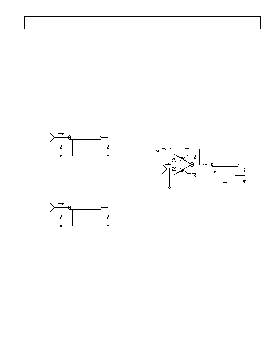
Analog Output
The analog output of the ADV7127 is a high impedance current
source. The current output is capable of directly driving a
37.5
load, such as a doubly terminated 75 coaxial cable.
Figure 22 shows the required configuration for the output con-
nected into a doubly terminated 75
load. This arrangement
will develop RS-343A video output voltage levels across a 75
monitor.
IOUT
ZO = 75
(CABLE)
ZS = 75
(SOURCE
TERMINATION)
ZL = 75
(MONITOR)
DAC
Figure 22. Analog Output Termination for RS-343A
A suggested method of driving RS-170 video levels into a 75
monitor is shown in Figure 23. The output current level of the
DAC remains unchanged, but the source termination resistance,
ZS, on the DAC is increased from 75
to 150 .
IOUT
ZO = 75
(CABLE)
ZS = 150
(SOURCE
TERMINATION)
ZL = 75
(MONITOR)
DAC
Figure 23. Analog Output Termination for RS-170
More detailed information regarding load terminations for vari-
ous output configurations, including RS-343A and RS-170, is
available in an Application Note entitled “Video Formats &
Required Load Terminations” available from Analog Devices,
publication no. E1228-15-1/89.
Figure 21 shows the video waveforms associated with the current
output driving the doubly terminated 75
load of Figure 22.
Gray Scale Operation
The ADV7127 can be used for stand-alone, gray scale (mono-
chrome) or composite video applications (i.e., only one channel
used for video information).
Video Output Buffer
The ADV7127 is specified to drive transmission line loads,
which is what most monitors are rated as. The analog output
configurations to drive such loads are described in the Analog
Interface section and illustrated in Figure 23. However, in some
applications it may be required to drive long “transmission line”
cable lengths. Cable lengths greater than 10 meters can attenu-
ate and distort high frequency analog output pulses. The inclu-
sion of output buffers will compensate for some cable distortion.
Buffers with large full power bandwidths and gains between two
and four will be required. These buffers will also need to be able
to supply sufficient current over the complete output voltage
swing. Analog Devices produces a range of suitable op amps for
such applications. These include the AD84x series of monolithic
op amps. In very high frequency applications (80 MHz), the
AD9617 is recommended. More information on line driver
buffering circuits is given in the relevant op amp data sheets.
Use of buffer amplifiers also allows implementation of other
video standards besides RS-343A and RS-170. Altering the gain
components of the buffer circuit will result in any desired
video level.
AD848
0.1 F
IOUT
Z1
Z2
ZO = 75
(CABLE)
ZS = 75
(SOURCE
TERMINATION)
ZL = 75
(MONITOR)
DAC
75
–VS
+VS
0.1 F
GAIN (G) = 1 +
Z1
Z2
Figure 24. AD848 As an Output Buffer
PC Board Layout Considerations
The ADV7127 is optimally designed for lowest noise perfor-
mance, both radiated and conducted noise. To complement the
excellent noise performance of the ADV7127 it is imperative
that great care be given to the PC board layout. Figure 25 shows
a recommended connection diagram for the ADV7127.
The layout should be optimized for lowest noise on the ADV7127
power and ground lines. This can be achieved by shielding the
digital inputs and providing good decoupling. The lead length
between groups of VAA and GND pins should be minimized to
inductive ringing.
Ground Planes
The ADV7127 and associated analog circuitry, should have a
separate ground plane referred to as the analog ground plane.
This ground plane should connect to the regular PCB ground
plane at a single point through a ferrite bead, as illustrated in
Figure 25. This bead should be located as close as possible
(within 3 inches) to the ADV7127.
The analog ground plane should encompass all ADV7127
ground pins, voltage reference circuitry, power supply bypass
circuitry, the analog output traces and any output amplifiers.
The regular PCB ground plane area should encompass all the
digital signal traces, excluding the ground pins, leading up to
the ADV7127.
相关PDF资料 |
PDF描述 |
|---|---|
| AD7243BNZ | IC DAC 12BIT AMP/REF 16DIP |
| MS27472T10B5PALC | CONN HSG RCPT 5POS WALL MT PINS |
| MS27474T12B98PLC | CONN HSG RCPT 10POS JAM NUT PINS |
| AD7845KPZ | IC DAC 12BIT MULT LC2MOS 28-PLCC |
| AD7245ABRZ | IC DAC 12BIT W/REF 24-SOIC |
相关代理商/技术参数 |
参数描述 |
|---|---|
| ADV7127JRZ240 | 制造商:Analog Devices 功能描述:DAC 1-CH Segment 10-bit 28-Pin SOIC W 制造商:Rochester Electronics LLC 功能描述:- Bulk 制造商:Analog Devices 功能描述:10Bit Tube |
| ADV7127KR140 | 制造商:Rochester Electronics LLC 功能描述:SINGLE HIGH SPEED VIDEO DAC I.C. - Bulk 制造商:Analog Devices 功能描述: |
| ADV7127KR140-REEL | 制造商:Analog Devices 功能描述:DAC 1-CH Segment 10-bit 28-Pin SOIC W T/R 制造商:Rochester Electronics LLC 功能描述:SINGLE HIGH SPEED VIDEO DAC I.C. - Tape and Reel |
| ADV7127KR50 | 制造商:Analog Devices 功能描述:DAC 1-CH Segment 10-bit 28-Pin SOIC W 制造商:Rochester Electronics LLC 功能描述:SINGLE HIGH SPEED VIDEO DAC I.C. - Bulk |
| ADV7127KR50-REEL | 制造商:Analog Devices 功能描述:DAC 1-CH Segment 10-bit 28-Pin SOIC W T/R 制造商:Rochester Electronics LLC 功能描述:SINGLE HIGH SPEED VIDEO DAC I.C. - Tape and Reel |
发布紧急采购,3分钟左右您将得到回复。