- 您现在的位置:买卖IC网 > PDF目录10971 > ADV7173KSTZ (Analog Devices Inc)IC DAC VIDEO NTSC 6-CH 48LQFP PDF资料下载
参数资料
| 型号: | ADV7173KSTZ |
| 厂商: | Analog Devices Inc |
| 文件页数: | 16/60页 |
| 文件大小: | 0K |
| 描述: | IC DAC VIDEO NTSC 6-CH 48LQFP |
| 标准包装: | 1 |
| 类型: | 视频编码器 |
| 应用: | 多媒体 |
| 电压 - 电源,模拟: | 4.75 V ~ 5.25 V |
| 安装类型: | 表面贴装 |
| 封装/外壳: | 48-LQFP |
| 供应商设备封装: | 48-LQFP(7x7) |
| 包装: | 托盘 |
| 产品目录页面: | 786 (CN2011-ZH PDF) |
第1页第2页第3页第4页第5页第6页第7页第8页第9页第10页第11页第12页第13页第14页第15页当前第16页第17页第18页第19页第20页第21页第22页第23页第24页第25页第26页第27页第28页第29页第30页第31页第32页第33页第34页第35页第36页第37页第38页第39页第40页第41页第42页第43页第44页第45页第46页第47页第48页第49页第50页第51页第52页第53页第54页第55页第56页第57页第58页第59页第60页
REV. B
ADV7172/ADV7173
–23–
POWER-ON RESET
After power-up, it is necessary to execute a reset operation. A
reset occurs on the falling edge of a high-to-low transition on
the
RESET pin. This initializes the pixel port such that the pixel
inputs P7–P0 are not selected. After reset, the ADV7172/
ADV7173 is automatically set up to operate in NTSC/PAL mode,
depending on the PAL_NTSC pin. The subcarrier frequency
registers are automatically loaded with the correct values for
PAL or NTSC. All other registers, with the exception of Mode
Registers 1 and 2, are set to 00H. Mode Register 1 is set to 07H.
This is to ensure DACs D, E, and F are ON after power-up.
All bits of Mode Register 2 are set to “0,” with the exception of
Bit 3 (i.e., Mode Register 2 reads 08H). Bit MR23 of Mode
Register 2 is set to Logic “1.” This enables the 7.5 IRE pedestal.
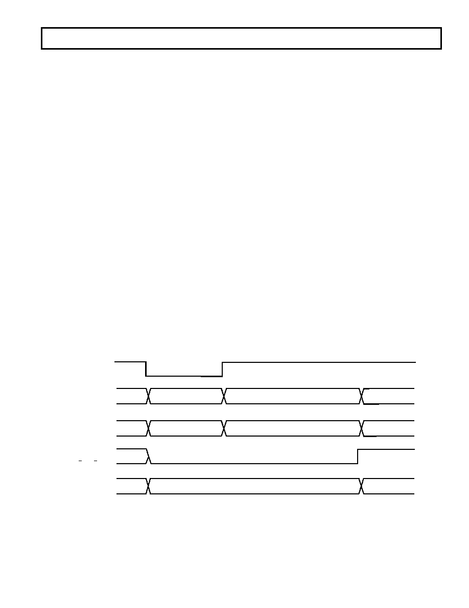
RESET SEQUENCE
When
RESET becomes active, the ADV7172/ADV7173 reverts
to the default output configuration. DACs A, B, C are off and
DACs D, E, F are powered on and output composite, luma and
chroma signals respectively. Mode Register 2, Bit 6 (MR26),
resets to “0.” The ADV7172/ADV7173 internal timing is under
the control of the logic level on the NTSC_PAL pin.
When
RESET is released Y, Cr, Cb values corresponding to a
black screen are input to the ADV7172/ADV7173. Output
timing signals are still suppressed at this stage.
When the user requires valid data, MR26 is set to “1” to allow
the valid pixel data to pass through the encoder. Digital output
timing signals become active and the encoder timing is now
under the control of the timing registers. If, at this stage, the
user wishes to select a video standard different from that on the
NTSC_PAL pin, Mode Register 2, Bit 5 (MR25) is set (“1”)
and the video standard required is selected by programming
Mode Register 0. Figure 36 illustrates the reset sequence timing.
SLEEP MODE
If after reset the SCRESET/RTC and NTSC_PAL pins are
both set to high, the part ADV7172/ADV7173 will power-up
in sleep mode to facilitate low power consumption before all
registers have been initialized. If Mode Register 6, Bit 0 (MR60) is
then set to (“1”) sleep mode control passes to Mode Register 2,
Bit 7 (i.e., control via I
2C).
SCH PHASE MODE
The SCH phase is configured in default mode to reset every
four (NTSC) or eight (PAL) fields to avoid an accumulation of
SCH phase error over time. In an ideal system, zero SCH phase
error would be maintained forever, but in reality, this is impos-
sible to achieve due to clock frequency variations. This effect is
reduced by the use of a 32-bit DDS, which generates this SCH.
Resetting the SCH phase every four or eight fields avoids the
accumulation of SCH phase error, and results in very minor
SCH phase jumps at the start of the four or eight field sequence.
Resetting the SCH phase should not be done if the video source
does not have stable timing or the ADV7172/ADV7173 is con-
figured in RTC mode (MR41 = “1” and MR42 = “1”). Under
these conditions (unstable video) the subcarrier phase reset should
be enabled (MR42 = “0” and MR41 = “1”) but no reset applied.
In this configuration the SCH phase will never be reset, which
that the output video will now track the unstable input video.
The subcarrier phase reset when applied will reset the SCH
phase to Field 0 at the start of the next field (e.g., subcarrier
phase reset applied in Field 5 (PAL) on the start of the next
field SCH phase will be reset to Field 0).
XXXXXXX
DIGITAL TIMING SIGNALS SUPPRESSED
BLACK VALUE
BLACK VALUE WITH SYNC
VALID VIDEO
0
1
TIMING ACTIVE
RESET
COMPOSITE/Y
CHROMA
MR26
PIXEL DATA VALID
DIGITAL TIMING
0
512
Figure 36.
RESET Sequence Timing Diagram
相关PDF资料 |
PDF描述 |
|---|---|
| VI-21M-IY-F3 | CONVERTER MOD DC/DC 10V 50W |
| VE-23V-IY-F4 | CONVERTER MOD DC/DC 5.8V 50W |
| VE-BTP-IX-B1 | CONVERTER MOD DC/DC 13.8V 75W |
| VE-BTP-IW-B1 | CONVERTER MOD DC/DC 13.8V 100W |
| AD725ARZ | IC ENCODER RGB TO NTSC 16-SOIC |
相关代理商/技术参数 |
参数描述 |
|---|---|
| ADV7173KSTZ-REEL | 功能描述:IC DAC VIDEO NTSC 6-CH 48LQFP RoHS:是 类别:集成电路 (IC) >> 接口 - 编码器,解码器,转换器 系列:- 产品变化通告:Development Systems Discontinuation 26/Apr/2011 标准包装:1 系列:- 类型:编码器 应用:DVB-S.2 系统 电压 - 电源,模拟:- 电压 - 电源,数字:- 安装类型:- 封装/外壳:模块 供应商设备封装:模块 包装:散装 其它名称:Q4645799 |
| ADV7174 | 制造商:AD 制造商全称:Analog Devices 功能描述:Chip Scale PAL/NTSC Video Encoder with Advanced Power Management |
| ADV7174BCP | 制造商:AD 制造商全称:Analog Devices 功能描述:Chip Scale PAL/NTSC Video Encoder with Advanced Power Management |
| ADV7174BCP-REEL | 制造商:AD 制造商全称:Analog Devices 功能描述:Chip Scale PAL/NTSC Video Encoder with Advanced Power Management |
| ADV7174KCP | 制造商:AD 制造商全称:Analog Devices 功能描述:Chip Scale PAL/NTSC Video Encoder with Advanced Power Management |
发布紧急采购,3分钟左右您将得到回复。