- 您现在的位置:买卖IC网 > PDF目录10971 > ADV7173KSTZ (Analog Devices Inc)IC DAC VIDEO NTSC 6-CH 48LQFP PDF资料下载
参数资料
| 型号: | ADV7173KSTZ |
| 厂商: | Analog Devices Inc |
| 文件页数: | 17/60页 |
| 文件大小: | 0K |
| 描述: | IC DAC VIDEO NTSC 6-CH 48LQFP |
| 标准包装: | 1 |
| 类型: | 视频编码器 |
| 应用: | 多媒体 |
| 电压 - 电源,模拟: | 4.75 V ~ 5.25 V |
| 安装类型: | 表面贴装 |
| 封装/外壳: | 48-LQFP |
| 供应商设备封装: | 48-LQFP(7x7) |
| 包装: | 托盘 |
| 产品目录页面: | 786 (CN2011-ZH PDF) |
第1页第2页第3页第4页第5页第6页第7页第8页第9页第10页第11页第12页第13页第14页第15页第16页当前第17页第18页第19页第20页第21页第22页第23页第24页第25页第26页第27页第28页第29页第30页第31页第32页第33页第34页第35页第36页第37页第38页第39页第40页第41页第42页第43页第44页第45页第46页第47页第48页第49页第50页第51页第52页第53页第54页第55页第56页第57页第58页第59页第60页
REV. B
ADV7172/ADV7173
–24–
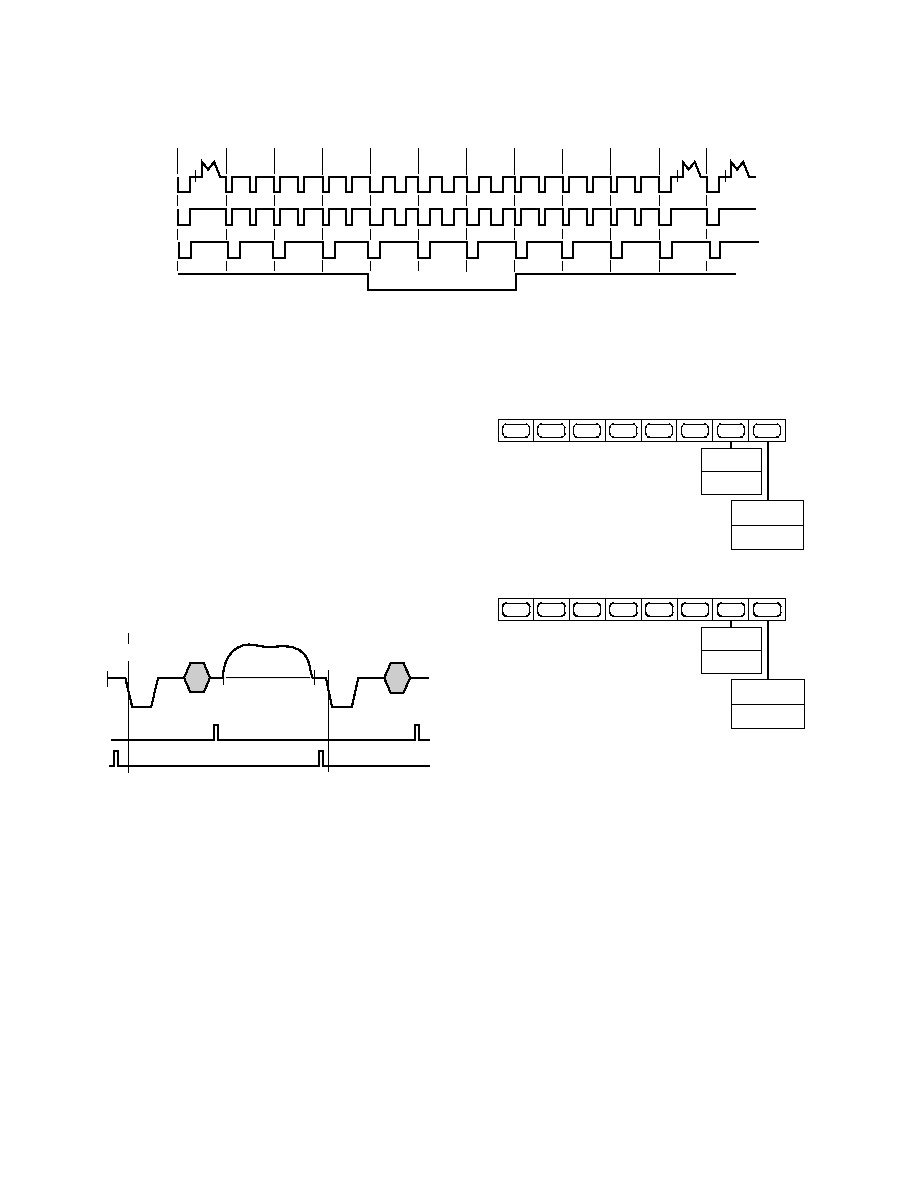
CSO, HSO, AND VSO OUTPUTS
The ADV7172/ADV7173 supports three timing signals,
CSO
(composite sync signal),
HSO (horizontal sync signal) and VSO
(vertical sync signal). These output TTL signals are aligned with
the analog video outputs.
HSO and CSO are shared on Pin 10.
Mode Register 7, Bit MR75 can be used to configure this out-
put pin. See Figure 37 for an example of these waveforms.
CLAMP OUTPUT
The ADV7172/ADV7173 has a programmable clamp TTL
output signal. The clamp signal is programmable to the front
and back porch. Mode Register 5, Bit MR57 can be used to
control the porch position. Also the position of the clamp signal
can be varied by 1–3 clock cycles in a positive and negative
direction from the default position. Mode Register 5, Bits MR56,
MR55, and MR54 control this position.
MR57 = 1
MR57 = 0
0H
Figure 38. Clamp Output Timing
MPU PORT DESCRIPTION
The ADV7172 and ADV7173 support a 2-wire serial (I
2C-
Compatible) microprocessor bus driving multiple peripherals.
Two inputs serial data (SDATA) and serial clock (SCLOCK)
carry information between any device connected to the bus.
Each slave device is recognized by a unique address. The
ADV7172 and ADV7173 each have four possible slave addresses
for both read and write operations. These are unique addresses
for each device and are illustrated in Figure 39 and Figure 40.
The LSB sets either a read or write operation. Logic Level
“1” corresponds to a read operation while Logic Level “0”
corresponds to a write operation. A1 is set by setting the ALSB
pin of the ADV7172/ADV7173 to Logic Level “0” or Logic
Level “1.” When ALSB is set to “0,” there is greater bandwidth
on the I
2C lines, which allows high-speed data transfers on this
bus. When ALSB is set to “1,” there is reduced input band-
width on the I
2C lines, which means that impulses of less
than 50 ns will not pass into the I
2C internal controller. This
mode is recommended for noisy systems.
ADDRESS
CONTROL
SET UP BY
ALSB
READ/WRITE
CONTROL
0
WRITE
1
READ
1
0
1
0
1
A1
X
Figure 39. ADV7172 Slave Address
ADDRESS
CONTROL
SET UP BY
ALSB
READ/WRITE
CONTROL
0
WRITE
1
READ
0
1
0
1
0
1
A1
X
Figure 40. ADV7173 Slave Address
To control the various devices on the bus the following protocol
must be followed. First the master initiates a data transfer by
establishing a start condition, defined by a high-to-low transition
on SDATA while SCLOCK remains high. This indicates that
an address/data stream will follow. All peripherals respond to
the Start condition and shift the next eight bits (7-bit address +
R/
W bit). The bits are transferred from MSB down to LSB. The
peripheral that recognizes the transmitted address responds by
pulling the data line low during the ninth clock pulse. This is
known as an acknowledge bit. All other devices withdraw from
the bus at this point and maintain an idle condition. The idle
condition is where the device monitors the SDATA and SCLOCK
lines waiting for the Start condition and the correct transmitted
address. The R/
W bit determines the direction of the data. A
Logic “0” on the LSB of the first byte means that the master
will write information to the peripheral. A Logic “1” on the LSB
of the first byte means that the master will read information
from the peripheral.
VSO
HSO
CSO
OUTPUT
VIDEO
525
123456789
10
11-19
EXAMPLE: NTSC
Figure 37.
CSO, HSO, VSO Timing Diagram
相关PDF资料 |
PDF描述 |
|---|---|
| VI-21M-IY-F3 | CONVERTER MOD DC/DC 10V 50W |
| VE-23V-IY-F4 | CONVERTER MOD DC/DC 5.8V 50W |
| VE-BTP-IX-B1 | CONVERTER MOD DC/DC 13.8V 75W |
| VE-BTP-IW-B1 | CONVERTER MOD DC/DC 13.8V 100W |
| AD725ARZ | IC ENCODER RGB TO NTSC 16-SOIC |
相关代理商/技术参数 |
参数描述 |
|---|---|
| ADV7173KSTZ-REEL | 功能描述:IC DAC VIDEO NTSC 6-CH 48LQFP RoHS:是 类别:集成电路 (IC) >> 接口 - 编码器,解码器,转换器 系列:- 产品变化通告:Development Systems Discontinuation 26/Apr/2011 标准包装:1 系列:- 类型:编码器 应用:DVB-S.2 系统 电压 - 电源,模拟:- 电压 - 电源,数字:- 安装类型:- 封装/外壳:模块 供应商设备封装:模块 包装:散装 其它名称:Q4645799 |
| ADV7174 | 制造商:AD 制造商全称:Analog Devices 功能描述:Chip Scale PAL/NTSC Video Encoder with Advanced Power Management |
| ADV7174BCP | 制造商:AD 制造商全称:Analog Devices 功能描述:Chip Scale PAL/NTSC Video Encoder with Advanced Power Management |
| ADV7174BCP-REEL | 制造商:AD 制造商全称:Analog Devices 功能描述:Chip Scale PAL/NTSC Video Encoder with Advanced Power Management |
| ADV7174KCP | 制造商:AD 制造商全称:Analog Devices 功能描述:Chip Scale PAL/NTSC Video Encoder with Advanced Power Management |
发布紧急采购,3分钟左右您将得到回复。