- 您现在的位置:买卖IC网 > PDF目录10973 > ADV7179BCPZ (Analog Devices Inc)IC ENCODER VID NTSC/PAL 40LFCSP PDF资料下载
参数资料
| 型号: | ADV7179BCPZ |
| 厂商: | Analog Devices Inc |
| 文件页数: | 18/52页 |
| 文件大小: | 0K |
| 描述: | IC ENCODER VID NTSC/PAL 40LFCSP |
| 产品培训模块: | Interfacing AV Converters to Blackfin Processors |
| 标准包装: | 1 |
| 类型: | 视频编码器 |
| 应用: | 数码相机,手机,便携式视频 |
| 电压 - 电源,模拟: | 2.8 V,3.3 V |
| 安装类型: | 表面贴装 |
| 封装/外壳: | 40-VFQFN 裸露焊盘,CSP |
| 供应商设备封装: | 40-LFCSP-VQ(6x6) |
| 包装: | 托盘 |
| 产品目录页面: | 786 (CN2011-ZH PDF) |
第1页第2页第3页第4页第5页第6页第7页第8页第9页第10页第11页第12页第13页第14页第15页第16页第17页当前第18页第19页第20页第21页第22页第23页第24页第25页第26页第27页第28页第29页第30页第31页第32页第33页第34页第35页第36页第37页第38页第39页第40页第41页第42页第43页第44页第45页第46页第47页第48页第49页第50页第51页第52页
ADV7174/ADV7179
Rev. B | Page 25 of 52
POWER-ON RESET
After power-up, it is necessary to execute a reset operation. A
reset occurs on the falling edge of a high-to-low transition on
the RESET pin. This initializes the pixel port so that the pixel
inputs, P7–P0, are selected. After reset, the ADV7174/ADV7179
are automatically set up to operate in NTSC mode. Subcarrier
frequency code 21F07C16H is loaded into the subcarrier
frequency registers. All other registers, with the exceptions of
Mode Register 1 and Mode Register 4, are set to 00H. Bit MR44
of Mode Register 4 is set to Logic 1. This enables the 7.5 IRE
pedestal. Bit MR13, DAC A, and Bit MR16, DAC C, are powered
down by default.
SCH PHASE MODE
The SCH phase is configured in default mode to reset every
four (NTSC) or eight (PAL) fields to avoid an accumulation of
SCH phase error over time. In an ideal system, 0 SCH phase
error would be maintained forever, but in reality, this is
impossible to achieve due to clock frequency variations. This
effect is reduced by the use of a 32-bit DDS, which generates
this SCH.
Resetting the SCH phase every four or eight fields avoids the
accumulation of SCH phase error and results in very minor
SCH phase jumps at the start of the 4- or 8-field sequence.
Resetting the SCH phase should not be done if the video source
does not have stable timing or the ADV7174/ADV7179 is
configured in RTC mode (MR21 = 1 and MR22 = 1). Under
these conditions (unstable video), the subcarrier phase reset
should be enabled (MR22 = 0 and MR21 = 1), but no reset
applied. In this configuration, the SCH phase can never be
reset, which means that the output video can now track the
unstable input video. The subcarrier phase reset, when applied,
resets the SCH phase to Field 0 at the start of the next field, for
example, subcarrier phase reset applied in Field 5 (PAL) on the
start of the next field SCH phase is reset to Field 0.
MPU PORT DESCRIPTION
The ADV7174/ADV7179 supports a 2-wire serial (I2C
compatible) microprocessor bus driving multiple peripherals.
Two inputs, serial data (SDATA) and serial clock (SCLOCK),
carry information between any device connected to the bus.
Each slave device is recognized by a unique address. The
ADV7174/ADV7179 has four possible slave addresses for both
read and write operations. These are unique addresses for each
sets either a read or write operation. Logic 1 corresponds to a
read operation, while Logic 0 corresponds to a write operation.
A 1 is set by setting the ALSB pin of the ADV7174/ ADV7179
to Logic 0 or Logic 1.
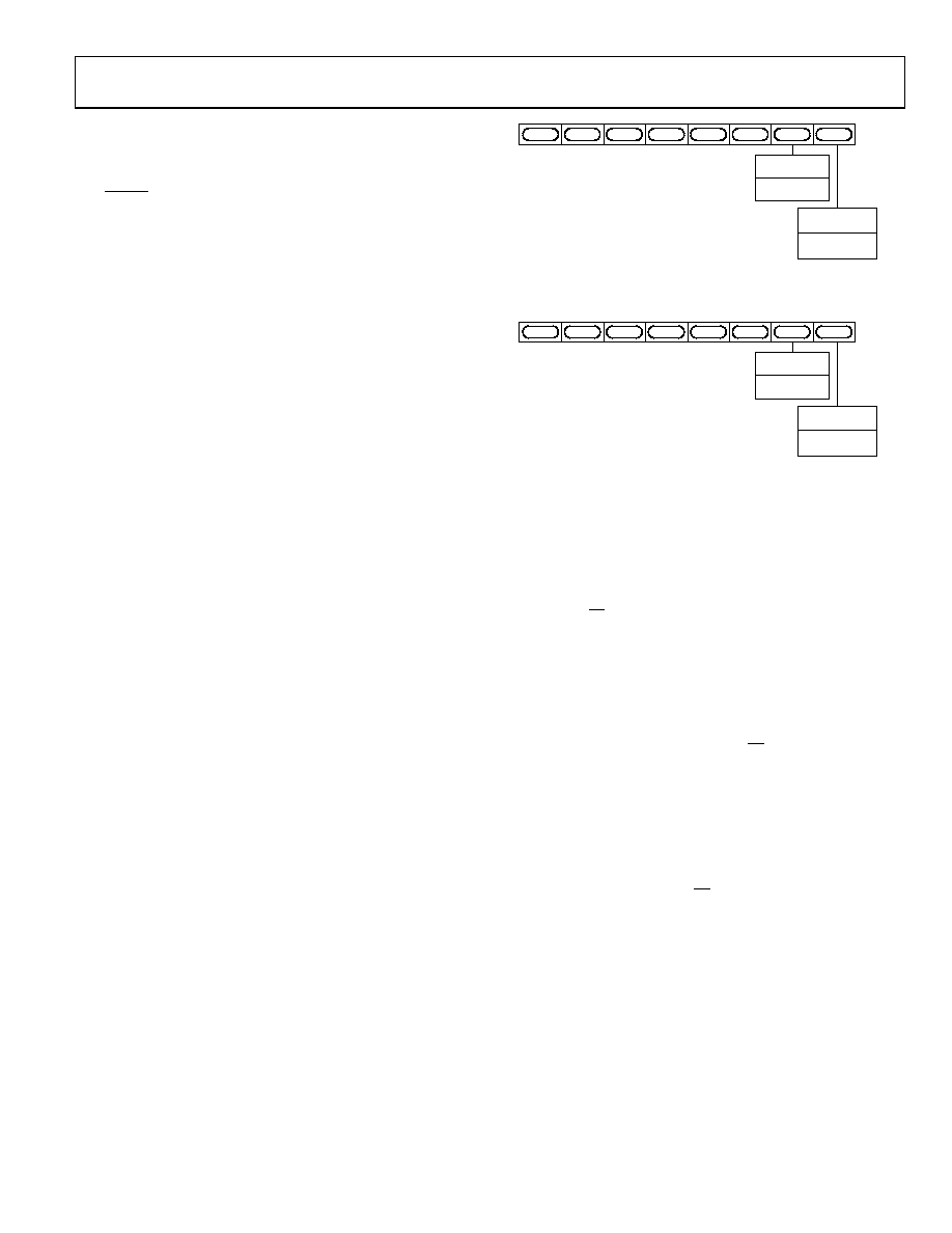
1
X
10
1
0
1
A1
ADDRESS
CONTROL
SET UP BY
ALSB
READ/WRITE
CONTROL
0
WRITE
1
READ
02980-
A-
032
Figure 33. ADV7174 Slave Address
0
X
10
1
0
1
A1
ADDRESS
CONTROL
SET UP BY
ALSB
READ/WRITE
CONTROL
0
WRITE
1
READ
02980-
A-
033
Figure 34. ADV7179 Slave Address
To control the various devices on the bus, the following
protocol must be followed: first, the master initiates a data
transfer by establishing a start condition, defined by a high-to-
low transition on SDATA while SCLOCK remains high. This
indicates that an address/data stream will follow. All peripherals
respond to the start condition and shift the next eight bits (7-bit
address + R/W bit). The bits transfer from MSB down to LSB.
The peripheral that recognizes the transmitted address
responds by pulling the data line low during the ninth clock
pulse. This is known as an Acknowledge bit. All other devices
withdraw from the bus at this point and maintain an idle
condition. The idle condition is where the device monitors the
SDATA and SCLOCK lines waiting for the start condition and
the correct transmitted address. The R/W bit determines the
direction of the data. A Logic 0 on the LSB of the first byte
means that the master will write information to the peripheral.
A Logic 1 on the LSB of the first byte means that the master will
read information from the peripheral.
The ADV7174/ADV7179 acts as a standard slave device on the
bus. The data on the SDATA pin is eight bits long, supporting
the 7-bit addresses plus the R/W bit. The ADV7174/ADV7179
has 26 subaddresses to enable access to the internal registers. It
therefore interprets the first byte as the device address and the
second byte as the starting subaddress. The subaddresses’ auto
increment allows data to be written to or read from the starting
subaddress. A data transfer is always terminated by a stop
condition. The user can also access any unique subaddress
register on a one-by-one basis without having to update all the
registers. There is one exception. The subcarrier frequency
registers should be updated in sequence, starting with
Subcarrier Frequency Register 0. The auto increment function
should then be used to increment and access Subcarrier
相关PDF资料 |
PDF描述 |
|---|---|
| VE-231-IY-F3 | CONVERTER MOD DC/DC 12V 50W |
| VE-B7L-IW-B1 | CONVERTER MOD DC/DC 28V 100W |
| CS4954-CQZ | IC VIDEO ENCODER NTSC/PAL 48TQFP |
| VE-230-IY-F4 | CONVERTER MOD DC/DC 5V 50W |
| VE-B7K-IX-B1 | CONVERTER MOD DC/DC 40V 75W |
相关代理商/技术参数 |
参数描述 |
|---|---|
| ADV7179BCPZ2 | 制造商:AD 制造商全称:Analog Devices 功能描述:Chip Scale PAL/NTSC Video Encoder with Advanced Power Management |
| ADV7179BCPZ-REEL | 制造商:Analog Devices 功能描述:Video Encoder 3DAC 10-Bit 40-Pin LFCSP EP T/R |
| ADV7179BCPZ-REEL2 | 制造商:AD 制造商全称:Analog Devices 功能描述:Chip Scale PAL/NTSC Video Encoder with Advanced Power Management |
| ADV7179KCP | 制造商:Analog Devices 功能描述:Video Encoder 3DAC 10-Bit 40-Pin LFCSP EP 制造商:Rochester Electronics LLC 功能描述:CHIP SCALE NTSC/PAL VID ENCODER APM I.C. - Bulk 制造商:Analog Devices 功能描述:IC VIDEO ENCODER |
| ADV7179KCP1 | 制造商:AD 制造商全称:Analog Devices 功能描述:Chip Scale PAL/NTSC Video Encoder with Advanced Power Management |
发布紧急采购,3分钟左右您将得到回复。