- 您现在的位置:买卖IC网 > PDF目录10973 > ADV7179BCPZ (Analog Devices Inc)IC ENCODER VID NTSC/PAL 40LFCSP PDF资料下载
参数资料
| 型号: | ADV7179BCPZ |
| 厂商: | Analog Devices Inc |
| 文件页数: | 9/52页 |
| 文件大小: | 0K |
| 描述: | IC ENCODER VID NTSC/PAL 40LFCSP |
| 产品培训模块: | Interfacing AV Converters to Blackfin Processors |
| 标准包装: | 1 |
| 类型: | 视频编码器 |
| 应用: | 数码相机,手机,便携式视频 |
| 电压 - 电源,模拟: | 2.8 V,3.3 V |
| 安装类型: | 表面贴装 |
| 封装/外壳: | 40-VFQFN 裸露焊盘,CSP |
| 供应商设备封装: | 40-LFCSP-VQ(6x6) |
| 包装: | 托盘 |
| 产品目录页面: | 786 (CN2011-ZH PDF) |
第1页第2页第3页第4页第5页第6页第7页第8页当前第9页第10页第11页第12页第13页第14页第15页第16页第17页第18页第19页第20页第21页第22页第23页第24页第25页第26页第27页第28页第29页第30页第31页第32页第33页第34页第35页第36页第37页第38页第39页第40页第41页第42页第43页第44页第45页第46页第47页第48页第49页第50页第51页第52页
ADV7174/ADV7179
Rev. B | Page 17 of 52
COMPOSITE
VIDEO
(e.g., VCR
OR CABLE)
HSYNC
FIELD/VSYNC
CLOCK
GREEN/LUMA/Y
RED/CHROMA/Pr
BLUE/COMPOSITE/Pb
AD7174/ADV7179
P7–P0
SCRESET/RTC
VIDEO
DECODER
(e.g., ADV7183A)
H/LTRANSITION
COUNT START
4 BITS
RESERVED
5 BITS
RESERVED
RESET
BIT3
SEQUENCE
BIT2
RESERVED
14 BITS
RESERVED
LOW
128
RTC
TIME SLOT: 01
14
67 68
NOT USED IN THE
ADV7174/ADV7179
19
VALID
SAMPLE
INVALID
SAMPLE
FSC PLL INCREMENT1
8/LLC
21
0
13
NOTES
1FSC PLL INCREMENT IS 22 BITS LONG, VALUE LOADED INTO ADV7174/ADV7179 FSC DDS REGISTER IS
FSC PLL INCREMENT BITS 21:0 PLUS BITS 0:9 OF THE SUBCARRIER FREQUENCY REGISTERS. ALL ZEROS SHOULD
BE WRITTEN TO THE SUBCARRIER FREQUENCY REGISTERS OF THE ADV7174/ADV7179.
2SEQUENCE BIT
PAL: 0 = LINE NORMAL, 1 = LINE INVERTED
NTSC: 0 = NO CHANGE
3RESET BIT
RESET ADV7174/ADV7179 DDS
0
02980-A
-019
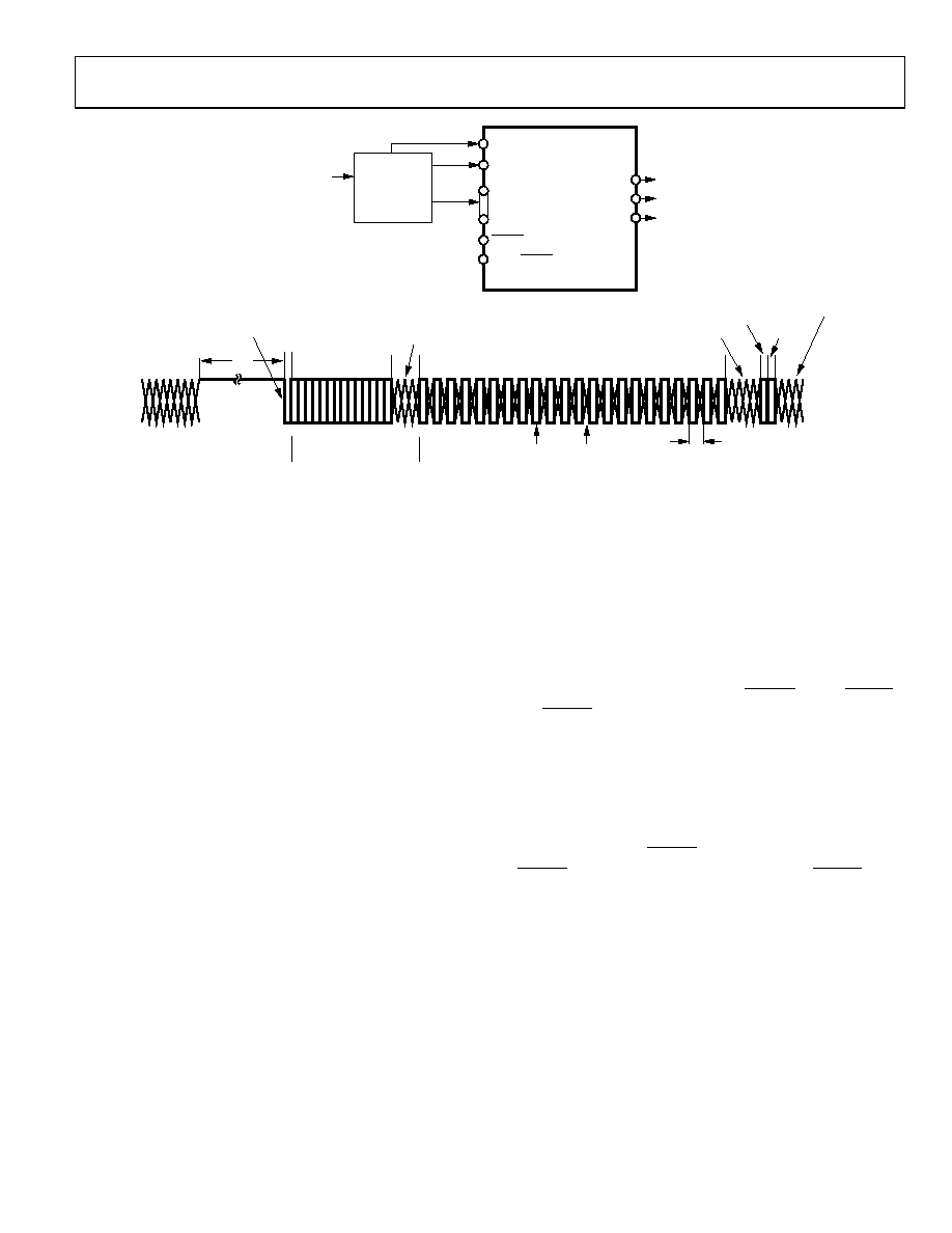
Figure 19. RTC Timing and Connections
Vertical Blanking Data Insertion
It is possible to allow encoding of incoming YCbCr data on
those lines of VBI that do not bear line sync or pre-/post-
operation is called partial blanking and is selected by setting
MR32 to 1. It allows the insertion of any VBI data (opened VBI)
into the encoded output waveform. This data is present in the
digitized incoming YCbCr data stream, for example. WSS data,
CGMS, VPS, and so on. Alternatively, the entire VBI may be
blanked (no VBI data inserted) on these lines by setting MR32
to 0.
Mode 0 (CCIR-656): Slave Option
(Timing Register 0 TR0 = X X X X X 0 0 0)
The ADV7174/ADV7179 is controlled by the SAV (start active
video) and EAV (end active video) time codes in the pixel data.
All timing information is transmitted using a 4-byte synchro-
nization pattern. A synchronization pattern is sent immediately
before and after each line during active picture and retrace.
Mode 0 is illustrated in Figure 20. The HSYNC, FIELD/VSYNC,
and BLANK (if not used) pins should be tied high during this
mode.
Mode 0 (CCIR-656): Master Option
(Timing Register 0 TR0 = X X X X X 0 0 1)
The ADV7174/ADV7179 generates H, V, and F signals required
for the SAV and EAV time codes in the CCIR-656 standard. The
H bit is output on the HSYNC pin, the V bit is output on the
BLANK pin, and the F bit is output on the FIELD/VSYNC pin.
Mode 0 is illustrated in
(NTSC) and
(PAL).
The H, V, and F transitions relative to the video waveform are
illustrated in
.
相关PDF资料 |
PDF描述 |
|---|---|
| VE-231-IY-F3 | CONVERTER MOD DC/DC 12V 50W |
| VE-B7L-IW-B1 | CONVERTER MOD DC/DC 28V 100W |
| CS4954-CQZ | IC VIDEO ENCODER NTSC/PAL 48TQFP |
| VE-230-IY-F4 | CONVERTER MOD DC/DC 5V 50W |
| VE-B7K-IX-B1 | CONVERTER MOD DC/DC 40V 75W |
相关代理商/技术参数 |
参数描述 |
|---|---|
| ADV7179BCPZ2 | 制造商:AD 制造商全称:Analog Devices 功能描述:Chip Scale PAL/NTSC Video Encoder with Advanced Power Management |
| ADV7179BCPZ-REEL | 制造商:Analog Devices 功能描述:Video Encoder 3DAC 10-Bit 40-Pin LFCSP EP T/R |
| ADV7179BCPZ-REEL2 | 制造商:AD 制造商全称:Analog Devices 功能描述:Chip Scale PAL/NTSC Video Encoder with Advanced Power Management |
| ADV7179KCP | 制造商:Analog Devices 功能描述:Video Encoder 3DAC 10-Bit 40-Pin LFCSP EP 制造商:Rochester Electronics LLC 功能描述:CHIP SCALE NTSC/PAL VID ENCODER APM I.C. - Bulk 制造商:Analog Devices 功能描述:IC VIDEO ENCODER |
| ADV7179KCP1 | 制造商:AD 制造商全称:Analog Devices 功能描述:Chip Scale PAL/NTSC Video Encoder with Advanced Power Management |
发布紧急采购,3分钟左右您将得到回复。