- 您现在的位置:买卖IC网 > PDF目录22035 > AGLN020V2-CSG81 (Microsemi SoC)IC FPGA 20K 1.2-1.5V CSP81 PDF资料下载
参数资料
| 型号: | AGLN020V2-CSG81 |
| 厂商: | Microsemi SoC |
| 文件页数: | 10/150页 |
| 文件大小: | 0K |
| 描述: | IC FPGA 20K 1.2-1.5V CSP81 |
| 标准包装: | 640 |
| 系列: | IGLOO nano |
| 逻辑元件/单元数: | 520 |
| 输入/输出数: | 52 |
| 门数: | 20000 |
| 电源电压: | 1.14 V ~ 1.575 V |
| 安装类型: | 表面贴装 |
| 工作温度: | -20°C ~ 70°C |
| 封装/外壳: | 81-WFBGA,CSBGA |
| 供应商设备封装: | 81-CSP(5x5) |
| 其它名称: | 1100-1124 |
第1页第2页第3页第4页第5页第6页第7页第8页第9页当前第10页第11页第12页第13页第14页第15页第16页第17页第18页第19页第20页第21页第22页第23页第24页第25页第26页第27页第28页第29页第30页第31页第32页第33页第34页第35页第36页第37页第38页第39页第40页第41页第42页第43页第44页第45页第46页第47页第48页第49页第50页第51页第52页第53页第54页第55页第56页第57页第58页第59页第60页第61页第62页第63页第64页第65页第66页第67页第68页第69页第70页第71页第72页第73页第74页第75页第76页第77页第78页第79页第80页第81页第82页第83页第84页第85页第86页第87页第88页第89页第90页第91页第92页第93页第94页第95页第96页第97页第98页第99页第100页第101页第102页第103页第104页第105页第106页第107页第108页第109页第110页第111页第112页第113页第114页第115页第116页第117页第118页第119页第120页第121页第122页第123页第124页第125页第126页第127页第128页第129页第130页第131页第132页第133页第134页第135页第136页第137页第138页第139页第140页第141页第142页第143页第144页第145页第146页第147页第148页第149页第150页
IGLOO nano Low Power Flash FPGAs
Revision 17
3-3
should be treated as a sensitive asynchronous signal. When defining pin placement and board layout,
simultaneously switching outputs (SSOs) and their effects on sensitive asynchronous pins must be
considered.
Unused FF or I/O pins are tristated with weak pull-up. This default configuration applies to both
Flash*Freeze mode and normal operation mode. No user intervention is required.
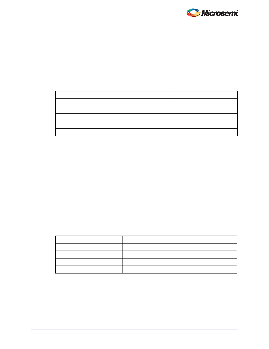
Table 3-1 shows the Flash*Freeze pin location on the available packages for IGLOO nano devices. The
Flash*Freeze pin location is independent of device (except for a PQ208 package), allowing migration to
larger or smaller IGLOO nano devices while maintaining the same pin location on the board. Refer to the
"Flash*Freeze Technology and Low Power Modes" chapter of the IGLOO nano FPGA Fabric User’s
Guide for more information on I/O states during Flash*Freeze mode.
JTAG Pins
Low power flash devices have a separate bank for the dedicated JTAG pins. The JTAG pins can be run
at any voltage from 1.5 V to 3.3 V (nominal). VCC must also be powered for the JTAG state machine to
operate, even if the device is in bypass mode; VJTAG alone is insufficient. Both VJTAG and VCC to the
part must be supplied to allow JTAG signals to transition the device. Isolating the JTAG power supply in a
separate I/O bank gives greater flexibility in supply selection and simplifies power supply and PCB
design. If the JTAG interface is neither used nor planned for use, the VJTAG pin together with the TRST
pin could be tied to GND.
TCK
Test Clock
Test clock input for JTAG boundary scan, ISP, and UJTAG. The TCK pin does not have an internal
pull-up/-down resistor. If JTAG is not used, Microsemi recommends tying off TCK to GND through a
resistor placed close to the FPGA pin. This prevents JTAG operation in case TMS enters an undesired
state.
Note that to operate at all VJTAG voltages, 500
to 1 k will satisfy the requirements. Refer to Table 3-2
for more information.
Table 3-1 Flash*Freeze Pin Locations for IGLOO nano Devices
Package
Flash*Freeze Pin
CS81/UC81
H2
QN48
14
QN68
18
VQ100
27
UC36
E2
Table 3-2 Recommended Tie-Off Values for the TCK and TRST Pins
VJTAG
Tie-Off Resistance 1,2
VJTAG at 3.3 V
200
to 1 k
VJTAG at 2.5 V
200
to 1 k
VJTAG at 1.8 V
500
to 1 k
VJTAG at 1.5 V
500
to 1 k
Notes:
1. The TCK pin can be pulled-up or pulled-down.
2. The TRST pin is pulled-down.
3. Equivalent parallel resistance if more than one device is on the JTAG chain
相关PDF资料 |
PDF描述 |
|---|---|
| ADM1026JST | IC CNTRL SYS REF/EEPROM 48LQFP |
| LQG15HSR22J02D | INDUCTOR 220NH 120MA 0402 |
| GCC10DCSN | CONN EDGECARD 20POS DIP .100 SLD |
| VJ1206Y122KBAAT4X | CAP CER 1200PF 50V 10% X7R 1206 |
| VI-B3X-CX | CONVERTER MOD DC/DC 5.2V 75W |
相关代理商/技术参数 |
参数描述 |
|---|---|
| AGLN020V2-CSG81I | 功能描述:IC FPGA NANO 1KB 20K 81-CSP RoHS:是 类别:集成电路 (IC) >> 嵌入式 - FPGA(现场可编程门阵列) 系列:IGLOO nano 标准包装:152 系列:IGLOO PLUS LAB/CLB数:- 逻辑元件/单元数:792 RAM 位总计:- 输入/输出数:120 门数:30000 电源电压:1.14 V ~ 1.575 V 安装类型:表面贴装 工作温度:-40°C ~ 85°C 封装/外壳:289-TFBGA,CSBGA 供应商设备封装:289-CSP(14x14) |
| AGLN020V2-QNG68 | 功能描述:IC FPGA 20K 1.2-1.5V 68QFN RoHS:是 类别:集成电路 (IC) >> 嵌入式 - FPGA(现场可编程门阵列) 系列:IGLOO nano 标准包装:60 系列:XP LAB/CLB数:- 逻辑元件/单元数:10000 RAM 位总计:221184 输入/输出数:244 门数:- 电源电压:1.71 V ~ 3.465 V 安装类型:表面贴装 工作温度:0°C ~ 85°C 封装/外壳:388-BBGA 供应商设备封装:388-FPBGA(23x23) 其它名称:220-1241 |
| AGLN020V2-QNG68I | 功能描述:IC FPGA NANO 1KB 20K 68-QFN RoHS:是 类别:集成电路 (IC) >> 嵌入式 - FPGA(现场可编程门阵列) 系列:IGLOO nano 标准包装:152 系列:IGLOO PLUS LAB/CLB数:- 逻辑元件/单元数:792 RAM 位总计:- 输入/输出数:120 门数:30000 电源电压:1.14 V ~ 1.575 V 安装类型:表面贴装 工作温度:-40°C ~ 85°C 封装/外壳:289-TFBGA,CSBGA 供应商设备封装:289-CSP(14x14) |
| AGLN020V2-UCG81 | 功能描述:IC FPGA NANO 1KB 20K 81-UCSP RoHS:是 类别:集成电路 (IC) >> 嵌入式 - FPGA(现场可编程门阵列) 系列:IGLOO nano 标准包装:152 系列:IGLOO PLUS LAB/CLB数:- 逻辑元件/单元数:792 RAM 位总计:- 输入/输出数:120 门数:30000 电源电压:1.14 V ~ 1.575 V 安装类型:表面贴装 工作温度:-40°C ~ 85°C 封装/外壳:289-TFBGA,CSBGA 供应商设备封装:289-CSP(14x14) |
| AGLN020V2-UCG81I | 功能描述:IC FPGA NANO 1KB 20K 81-UCSP RoHS:是 类别:集成电路 (IC) >> 嵌入式 - FPGA(现场可编程门阵列) 系列:IGLOO nano 标准包装:152 系列:IGLOO PLUS LAB/CLB数:- 逻辑元件/单元数:792 RAM 位总计:- 输入/输出数:120 门数:30000 电源电压:1.14 V ~ 1.575 V 安装类型:表面贴装 工作温度:-40°C ~ 85°C 封装/外壳:289-TFBGA,CSBGA 供应商设备封装:289-CSP(14x14) |
发布紧急采购,3分钟左右您将得到回复。