参数资料
| 型号: | AGLP030V2-CS289 |
| 厂商: | Microsemi SoC |
| 文件页数: | 45/134页 |
| 文件大小: | 0K |
| 描述: | IC FPGA IGLOO PLUS 30K 289-CSP |
| 标准包装: | 152 |
| 系列: | IGLOO PLUS |
| 逻辑元件/单元数: | 792 |
| 输入/输出数: | 120 |
| 门数: | 30000 |
| 电源电压: | 1.14 V ~ 1.575 V |
| 安装类型: | 表面贴装 |
| 工作温度: | 0°C ~ 70°C |
| 封装/外壳: | 289-TFBGA,CSBGA |
| 供应商设备封装: | 289-CSP(14x14) |
第1页第2页第3页第4页第5页第6页第7页第8页第9页第10页第11页第12页第13页第14页第15页第16页第17页第18页第19页第20页第21页第22页第23页第24页第25页第26页第27页第28页第29页第30页第31页第32页第33页第34页第35页第36页第37页第38页第39页第40页第41页第42页第43页第44页当前第45页第46页第47页第48页第49页第50页第51页第52页第53页第54页第55页第56页第57页第58页第59页第60页第61页第62页第63页第64页第65页第66页第67页第68页第69页第70页第71页第72页第73页第74页第75页第76页第77页第78页第79页第80页第81页第82页第83页第84页第85页第86页第87页第88页第89页第90页第91页第92页第93页第94页第95页第96页第97页第98页第99页第100页第101页第102页第103页第104页第105页第106页第107页第108页第109页第110页第111页第112页第113页第114页第115页第116页第117页第118页第119页第120页第121页第122页第123页第124页第125页第126页第127页第128页第129页第130页第131页第132页第133页第134页
IGLOO PLUS DC and Switching Characteristics
2-4
Revision 16
PLL Behavior at Brownout Condition
Microsemi recommends using monotonic power supplies or voltage regulators to ensure proper power-
up behavior. Power ramp-up should be monotonic at least until VCC and VCCPLX exceed brownout
activation levels (see Figure 2-1 and Figure 2-2 on page 2-5 for more details).
When PLL power supply voltage and/or VCC levels drop below the VCC brownout levels (0.75 V ± 0.25
V for V5 devices, and 0.75 V ± 0.2 V for V2 devices), the PLL output lock signal goes Low and/or the
output clock is lost. Refer to the "Brownout Voltage" section in the "Power-Up/-Down Behavior of Low
Power Flash Devices" chapter of the IGLOO PLUS Device Family User’s Guide for information on clock
and lock recovery.
Internal Power-Up Activation Sequence
1. Core
2. Input buffers
3. Output buffers, after 200 ns delay from input buffer activation
To make sure the transition from input buffers to output buffers is clean, ensure that there is no path
longer than 100 ns from input buffer to output buffer in your design.
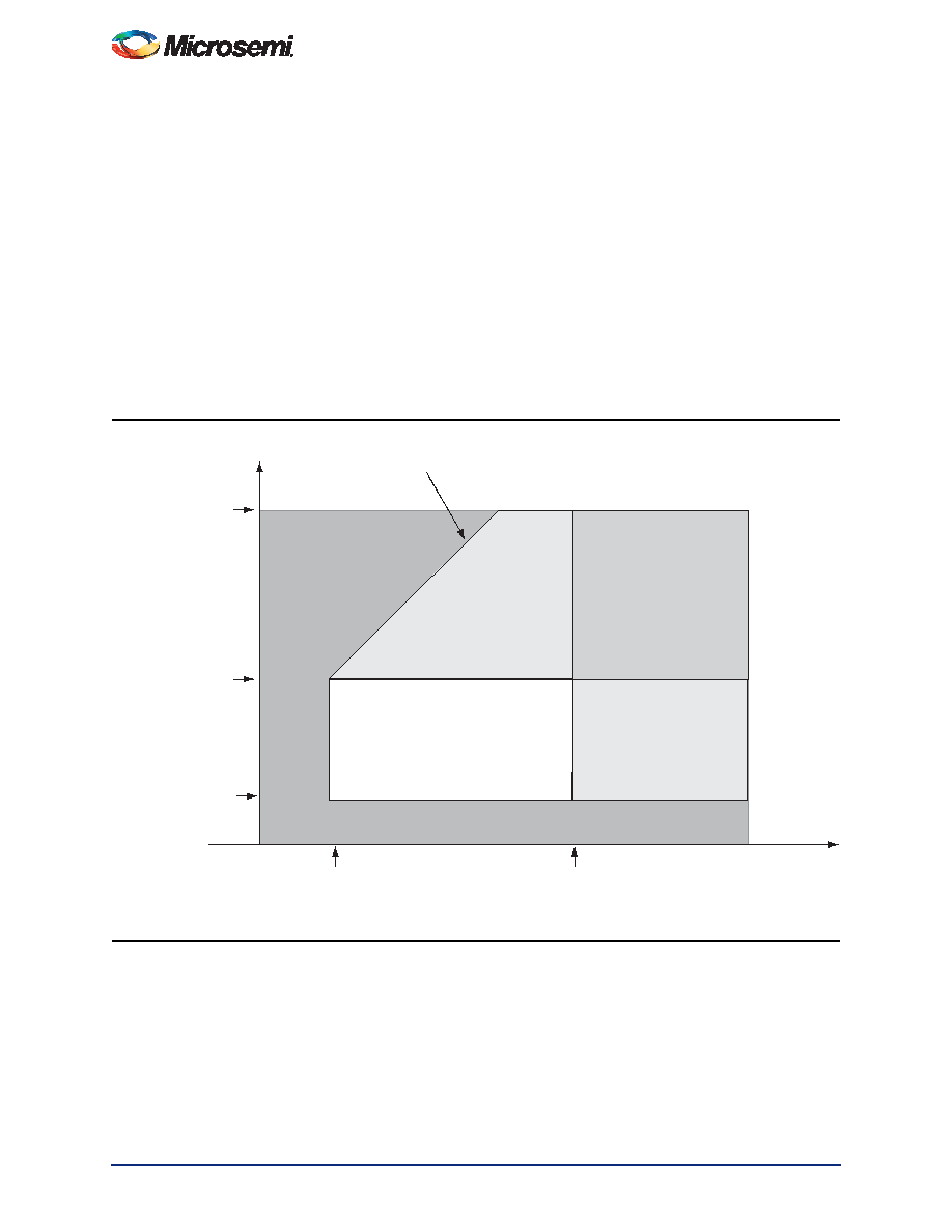
Figure 2-1 V5 Devices – I/O State as a Function of VCCI and VCC Voltage Levels
Region 1: I/O buffers are OFF
Region 2: I/O buffers are ON.
I/Os are functional (except differential inputs)
but slower because VCCI / VCC are below
specification. For the same reason, input
buffers do not meet VIH / VIL levels, and
output buffers do not meet VOH / VOL levels.
Min VCCI datasheet specification
voltage at a selected I/O
standard; i.e., 1.425 V or 1.7 V
or 2.3 V or 3.0 V
VCC
VCC = 1.425 V
Region 1: I/O Buffers are OFF
Activation trip point:
Va = 0.85 V ± 0.25 V
Deactivation trip point:
Vd = 0.75 V ± 0.25 V
Activation trip point:
Va = 0.9 V ± 0.3 V
Deactivation trip point:
Vd = 0.8 V ± 0.3 V
VCC = 1.575 V
Region 5: I/O buffers are ON
and power supplies are within
specification.
I/Os meet the entire datasheet
and timer specifications for
speed, VIH / VIL, VOH / VOL,
etc.
Region 4: I/O
buffers are ON.
I/Os are functional
(except differential
but slower because VCCI
is below specification. For the
same reason, input buffers do not
meet VIH / VIL levels, and output
buffers do not meet VOH / VOL levels.
Region 4: I/O
buffers are ON.
I/Os are functional
(except differential inputs)
where VT can be from 0.58 V to 0.9 V (typically 0.75 V)
VCCI
Region 3: I/O buffers are ON.
I/Os are functional; I/O DC
specifications are met,
but I/Os are slower because
the VCC is below specification.
VCC = VCCI + VT
相关PDF资料 |
PDF描述 |
|---|---|
| GEC40DTEI | CONN EDGECARD 80POS .100 EYELET |
| GSC65DRYN | CONN EDGECARD 130PS DIP .100 SLD |
| BR24T256FVT-WE2 | IC EEPROM I2C 256K 400KHZ 8TSSOP |
| GMC65DRYN | CONN EDGECARD 130PS DIP .100 SLD |
| GSC65DRYH | CONN EDGECARD 130PS DIP .100 SLD |
相关代理商/技术参数 |
参数描述 |
|---|---|
| AGLP030-V2CS289ES | 制造商:ACTEL 制造商全称:Actel Corporation 功能描述:IGLOO PLUS Low-Power Flash FPGAs with FlashFreeze Technology |
| AGLP030-V2CS289I | 制造商:ACTEL 制造商全称:Actel Corporation 功能描述:IGLOO PLUS Low-Power Flash FPGAs with FlashFreeze Technology |
| AGLP030V2-CS289I | 功能描述:IC FPGA IGLOO PLUS 30K 289-CSP RoHS:否 类别:集成电路 (IC) >> 嵌入式 - FPGA(现场可编程门阵列) 系列:IGLOO PLUS 标准包装:152 系列:IGLOO PLUS LAB/CLB数:- 逻辑元件/单元数:792 RAM 位总计:- 输入/输出数:120 门数:30000 电源电压:1.14 V ~ 1.575 V 安装类型:表面贴装 工作温度:-40°C ~ 85°C 封装/外壳:289-TFBGA,CSBGA 供应商设备封装:289-CSP(14x14) |
| AGLP030-V2CS289PP | 制造商:ACTEL 制造商全称:Actel Corporation 功能描述:IGLOO PLUS Low-Power Flash FPGAs with FlashFreeze Technology |
| AGLP030V2-CSG201 | 功能描述:IC FPGA IGLOO PLUS 30K 201-CSP RoHS:是 类别:集成电路 (IC) >> 嵌入式 - FPGA(现场可编程门阵列) 系列:IGLOO PLUS 标准包装:152 系列:IGLOO PLUS LAB/CLB数:- 逻辑元件/单元数:792 RAM 位总计:- 输入/输出数:120 门数:30000 电源电压:1.14 V ~ 1.575 V 安装类型:表面贴装 工作温度:-40°C ~ 85°C 封装/外壳:289-TFBGA,CSBGA 供应商设备封装:289-CSP(14x14) |
发布紧急采购,3分钟左右您将得到回复。