- 您现在的位置:买卖IC网 > PDF目录92914 > AH31 (TRIQUINT SEMICONDUCTOR INC) 50 MHz - 500 MHz RF/MICROWAVE WIDE BAND MEDIUM POWER AMPLIFIER PDF资料下载
参数资料
| 型号: | AH31 |
| 厂商: | TRIQUINT SEMICONDUCTOR INC |
| 元件分类: | 放大器 |
| 英文描述: | 50 MHz - 500 MHz RF/MICROWAVE WIDE BAND MEDIUM POWER AMPLIFIER |
| 封装: | TO-243C, SOT-89, 3 PIN |
| 文件页数: | 3/8页 |
| 文件大小: | 486K |
| 代理商: | AH31 |
Specifications and information are subject to change without notice
WJ Communications, Inc
Phone 1-800-WJ1-4401
FAX: 408-577-6621
e-mail: sales@wj.com
Web site: www.wj.com
Page 3 of 8 June 2005
AH31
High Dynamic Range IF Amplifier
Product Information
The Communications Edge TM
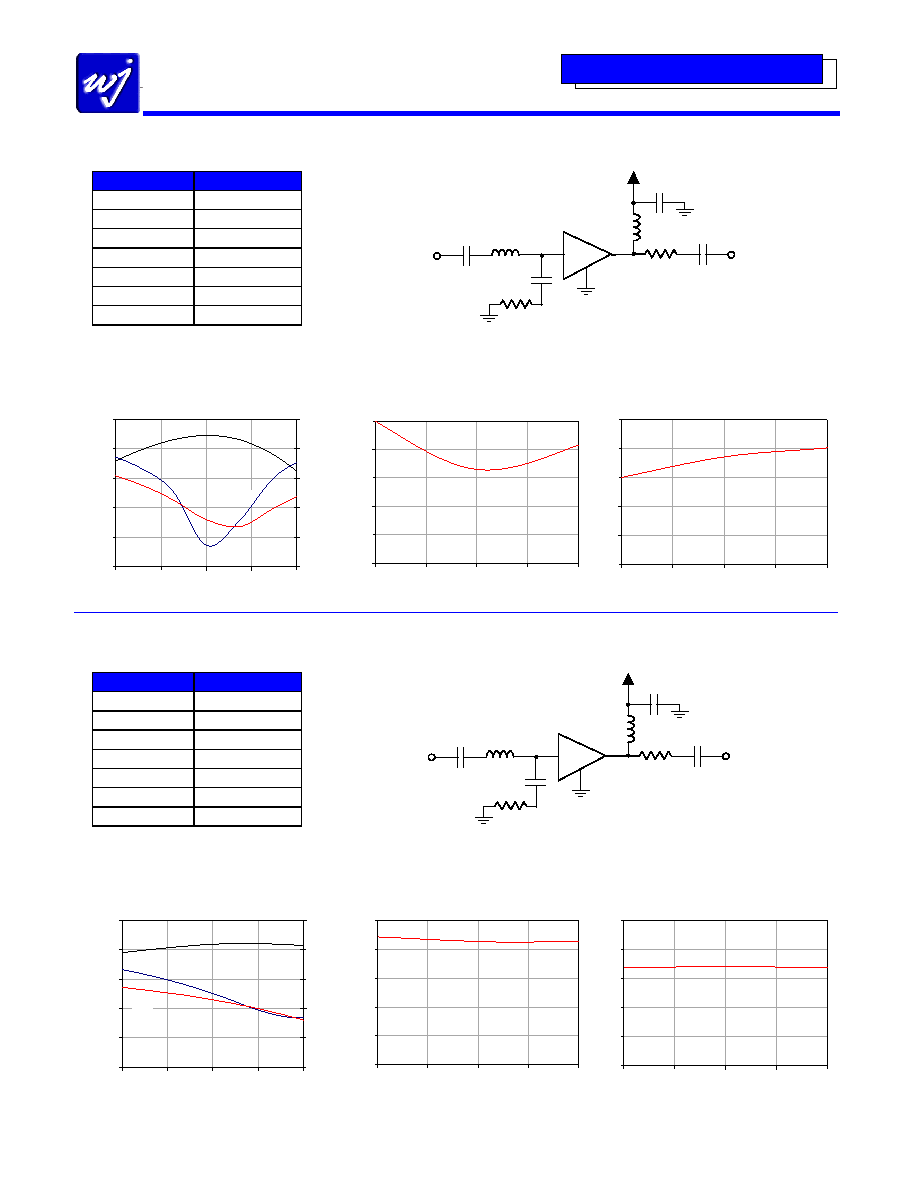
Application Circuit: 65 – 85 MHz (AH31-PCB75)
Typical Performance
Frequency
75 MHz
Gain
19.5 dB
S11
-21 dB
S22
-17 dB
Output P1dB
+22 dBm
Output IP3
+42 dBm
Noise Figure
2.6 dB
Bias
+5 V @ 150 mA
Notes:
1. The amplifier should be connected directly to a +5 V regulator; no dropping resistor is required.
2. If no DC signal is present at the input (pin 1), C1 can be removed. The gate is internally grounded in the amplifier.
3. R2 is used as a placeholder for a different application circuit. It can be removed from the circuit.
4. C2 (from the silkscreen) is not utilized in this application circuit.
S-Parameters
15
16
17
18
19
20
55
65
75
85
95
Frequency (MHz)
G
a
in
(d
B
)
-25
-20
-15
-10
-5
0
S
1
,
S
2
(d
B
)
S11
S22
S21
Noise Figure
1
1.5
2
2.5
3
3.5
55
65
75
85
95
Frequency (MHz)
N
o
is
e
F
ig
u
re
(d
B
)
Output IP3
36
38
40
42
44
46
55
65
75
85
95
Frequency (MHz)
O
u
tp
u
t
IP
3
(d
B
m
)
Application Circuit: 155 – 185 MHz (AH31-PCB170)
Typical Performance
Frequency
170 MHz
Gain
19.2 dB
S11
-13 dB
S22
-14 dB
Output P1dB
+21 dBm
Output IP3
+42 dBm
Noise Figure
2.3 dB
Bias
+5 V @ 150 mA
Notes:
1. The amplifier should be connected directly to a +5 V regulator; no dropping resistor is required.
2. If no DC signal is present at the input (pin 1), C1 can be removed. The gate is internally grounded in the amplifier.
3. R2 is used as a placeholder for a different application circuit. It can be removed from the circuit.
4. C2 (from the silkscreen) is not utilized in this application circuit.
S-Parameters
15
16
17
18
19
20
150
160
170
180
190
Frequency (MHz)
G
a
in
(d
B
)
-25
-20
-15
-10
-5
0
S
1
,
S
2
(d
B
)
S11
S22
S21
Noise Figure
0.0
0.5
1.0
1.5
2.0
2.5
150
160
170
180
190
Frequency (MHz)
N
o
is
e
F
ig
u
re
(d
B
)
Output IP3
36
38
40
42
44
46
150
160
170
180
190
Frequency (MHz)
O
u
tp
u
t
IP
3
(d
B
m
)
AH31
RF
VS = +5 V
C5
.018
F
L1
220 nH
C4
.018
F
L2
330 nH
RF IN
R1
5.1
§
C3
12 pF
C1
.018
F
R2
0
¨
AH31
RF
VS = +5 V
C5
.018
F
L1
82 nH
C4
1000 pF
L2
330 nH
RF IN
R1
3.3
§
C3
4.7 pF
C1
1000 pF
R2
0
¨
相关PDF资料 |
PDF描述 |
|---|---|
| AH31 | 50 MHz - 500 MHz RF/MICROWAVE WIDE BAND MEDIUM POWER AMPLIFIER |
| AH4 | 250 MHz - 6000 MHz RF/MICROWAVE WIDE BAND MEDIUM POWER AMPLIFIER |
| AHAMC | MOBILE STATION ANTENNA |
| AB144/440C | MOBILE STATION ANTENNA |
| ADB140 | MOBILE STATION ANTENNA |
相关代理商/技术参数 |
参数描述 |
|---|---|
| AH3100B4W | 制造商:Cooper Wiring Devices 功能描述: |
| AH3100C4W | 制造商:Cooper Wiring Devices 功能描述: |
| AH31-1 | 制造商:未知厂家 制造商全称:未知厂家 功能描述:Analog IC |
| AH312 | 制造商:未知厂家 制造商全称:未知厂家 功能描述:InGaP HBT Amplifiers |
| AH312-RFID | 制造商:WJCI 制造商全称:WJCI 功能描述:2 Watt, High Linearity InGaP HBT Amplifier |
发布紧急采购,3分钟左右您将得到回复。