- 您现在的位置:买卖IC网 > Datasheet目录393 > ALD1101BPAL (Advanced Linear Devices Inc)MOSFET 2N-CH 13.2V 40MA 8PDIP Datasheet资料下载
参数资料
| 型号: | ALD1101BPAL |
| 厂商: | Advanced Linear Devices Inc |
| 文件页数: | 1/8页 |
| 文件大小: | 0K |
| 描述: | MOSFET 2N-CH 13.2V 40MA 8PDIP |
| 标准包装: | 50 |
| FET 型: | 2 个 N 沟道(双) |
| FET 特点: | 标准 |
| 漏极至源极电压(Vdss): | 13.2V |
| 电流 - 连续漏极(Id) @ 25° C: | 40mA |
| 开态Rds(最大)@ Id, Vgs @ 25° C: | 75 欧姆 @ 5V |
| Id 时的 Vgs(th)(最大): | 1V @ 10µA |
| 功率 - 最大: | 500mW |
| 安装类型: | 通孔 |
| 封装/外壳: | 8-DIP(0.300",7.62mm) |
| 供应商设备封装: | 8-PDIP |
| 包装: | 管件 |
�� �
�
�A� DVANCED�
�L� INEAR�
�D� EVICES,� I� NC.�
�GENERAL� DESCRIPTION�
�DUAL� N-CHANNEL� MATCHED� MOSFET� PAIR�
�APPLICATIONS�
�ALD1101A/ALD1101B�
�ALD1101�
�The� ALD1101� is� a� monolithic� dual� N-channel� matched� transistor� pair�
�intended� for� a� broad� range� of� analog� applications.� These� enhancement-�
�mode� transistors� are� manufactured� with� Advanced� Linear� Devices'� en-�
�hanced� ACMOS� silicon� gate� CMOS� process.�
�The� ALD1101� offers� high� input� impedance� and� negative� current� tempera-�
�ture� coefficient.� The� transistor� pair� is� matched� for� minimum� offset� voltage�
�and� differential� thermal� response,� and� it� is� designed� for� switching� and�
�amplifying� applications� in� +2V� to� +12V� systems� where� low� input� bias�
�current,� low� input� capacitance� and� fast� switching� speed� are� desired.� Since�
�these� are� MOSFET� devices,� they� feature� very� large� (almost� infinite)�
�current� gain� in� a� low� frequency,� or� near� DC,� operating� environment.� When�
�used� with� an� ALD1102,� a� dual� CMOS� analog� switch� can� be� constructed.�
�?�
�?�
�?�
�?�
�?�
�?�
�?�
�?�
�?�
�Precision� current� mirrors�
�Precision� current� sources�
�Analog� switches�
�Choppers�
�Differential� amplifier� input� stage�
�Voltage� comparator�
�Data� converters�
�Sample� and� Hold�
�Analog� inverter�
�In� addition,� the� ALD1101� is� intended� as� a� building� block� for� differential�
�amplifier� input� stages,� transmission� gates,� and� multiplexer� applications.�
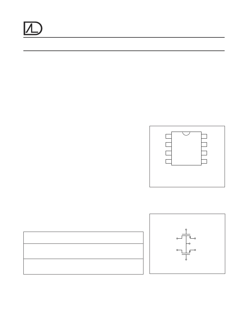
�PIN� CONFIGURATION�
�The� ALD1101� is� suitable� for� use� in� precision� applications� which� require�
�very� high� current� gain,� beta,� such� as� current� mirrors� and� current� sources.�
�The� high� input� impedance� and� the� high� DC� current� gain� of� the� Field� Effect�
�SOURCE� 1�
�GATE� 1�
�1�
�2�
�8�
�7�
�SUBSTRATE�
�SOURCE� 2�
�Transistors� result� in� extremely� low� current� loss� through� the� control� gate.�
�The� DC� current� gain� is� limited� by� the� gate� input� leakage� current,� which� is�
�DRAIN� 1�
�3�
�6�
�GATE� 2�
�specified� at� 50pA� at� room� temperature.� For� example,� DC� beta� of� the� device�
�at� a� drain� current� of� 5mA� at� 25� °� C� is� =� 5mA/50pA� =� 100,000,000.�
�IC�
�4�
�5�
�DRAIN� 2�
�TOP� VIEW�
�FEATURES�
�?� Low� threshold� voltage� of� 0.7V�
�?� Low� input� capacitance�
�?� Low� Vos� grades� --� 2mV,� 5mV,� 10mV�
�?� High� input� impedance� --� 10� 12� ?� typical�
�?� Negative� current� (I� DS� )� temperature� coefficient�
�?� Enhancement-mode� (normally� off)�
�?� DC� current� gain� 10� 9�
�?� RoHS� compliant�
�ORDERING� INFORMATION� (“L”� suffix� denotes� lead-free� (RoHS))�
�Operating� Temperature� Range�
�SAL,� PAL,� DA� PACKAGES�
�*� IC� pin� is� internally� connected.� Do� not� connect� externally.�
�BLOCK� DIAGRAM�
�GATE� 1� (2)�
�0� °� C� to� +70� °� C�
�0� °� C� to� +70� °� C� -55� °� C� to� +125� °� C�
�DRAIN� 1� (3)�
�SOURCE� 1� (1)�
�SUBSTRATE� (8)�
�8-Pin�
�8-Pin�
�8-Pin�
�Small� Outline�
�Plastic� Dip�
�CERDIP�
�DRAIN� 2� (5)�
�SOURCE� 2� (7)�
�Package� (SOIC)�
�ALD1101ASAL�
�ALD1101BSAL�
�ALD1101SAL�
�Package�
�ALD1101APAL�
�ALD1101BPAL�
�ALD1101PAL�
�Package�
�ALD1101DA�
�GATE� 2� (6)�
�*� Contact� factory� for� leaded� (non-RoHS)� or� high� temperature� versions.�
�Rev� 2.1� ?2012� Advanced� Linear� Devices,� Inc.� 415� Tasman� Drive,� Sunnyvale,� CA� 94089-1706� Tel:� (408)� 747-1155� Fax:� (408)� 747-1286�
�www.aldinc.com�
�相关PDF资料 |
PDF描述 |
|---|---|
| ALD1102BPAL | MOSFET 2P-CH 13.2V 16MA 8PDIP |
| ALD1103PBL | MOSFET 2N+2P 13.2V 14PDIP |
| ALD1105PBL | MOSFET 2N+2P 13.2V 14PDIP |
| ALD1106SBL | MOSFET 4N-CH 13.2V QUAD 14SOIC |
| ALD1107SBL | MOSFET 4P-CH 13.2V QUAD 14SOIC |
相关代理商/技术参数 |
参数描述 |
|---|---|
| ALD1101BSAL | 功能描述:MOSFET Dual N-Ch FET 10.6 500mW 0.7V 10Ohm RoHS:否 制造商:STMicroelectronics 晶体管极性:N-Channel 汲极/源极击穿电压:650 V 闸/源击穿电压:25 V 漏极连续电流:130 A 电阻汲极/源极 RDS(导通):0.014 Ohms 配置:Single 最大工作温度: 安装风格:Through Hole 封装 / 箱体:Max247 封装:Tube |
| ALD1101DA | 制造商:ALD 制造商全称:Advanced Linear Devices 功能描述:DUAL N-CHANNEL MATCHED MOSFET PAIR |
| ALD1101MA | 制造商:未知厂家 制造商全称:未知厂家 功能描述:TRANSISTOR | MOSFET | MATCHED PAIR | N-CHANNEL | 13.2V V(BR)DSS | TO-99 |
| ALD1101PA | 功能描述:MOSFET Dual N-Channel Pair RoHS:否 制造商:STMicroelectronics 晶体管极性:N-Channel 汲极/源极击穿电压:650 V 闸/源击穿电压:25 V 漏极连续电流:130 A 电阻汲极/源极 RDS(导通):0.014 Ohms 配置:Single 最大工作温度: 安装风格:Through Hole 封装 / 箱体:Max247 封装:Tube |
| ALD1101PAL | 功能描述:MOSFET Dual N-Channel Pair RoHS:否 制造商:STMicroelectronics 晶体管极性:N-Channel 汲极/源极击穿电压:650 V 闸/源击穿电压:25 V 漏极连续电流:130 A 电阻汲极/源极 RDS(导通):0.014 Ohms 配置:Single 最大工作温度: 安装风格:Through Hole 封装 / 箱体:Max247 封装:Tube |
发布紧急采购,3分钟左右您将得到回复。