- 您现在的位置:买卖IC网 > PDF目录166214 > AM29F400BB-120SD (SPANSION LLC) Flash Memory IC; Leaded Process Compatible:Yes; Memory Size:4Mbit; Package/Case:44-SOIC; Peak Reflow Compatible (260 C):Yes; Supply Voltage Max:5V; Access Time, Tacc:120ns; Series:AM29 RoHS Compliant: Yes PDF资料下载
参数资料
| 型号: | AM29F400BB-120SD |
| 厂商: | SPANSION LLC |
| 元件分类: | PROM |
| 英文描述: | Flash Memory IC; Leaded Process Compatible:Yes; Memory Size:4Mbit; Package/Case:44-SOIC; Peak Reflow Compatible (260 C):Yes; Supply Voltage Max:5V; Access Time, Tacc:120ns; Series:AM29 RoHS Compliant: Yes |
| 中文描述: | 256K X 16 FLASH 5V PROM, 120 ns, PDSO44 |
| 封装: | LEAD FREE, MO-180AA, SOP-44 |
| 文件页数: | 13/43页 |
| 文件大小: | 865K |
| 代理商: | AM29F400BB-120SD |
第1页第2页第3页第4页第5页第6页第7页第8页第9页第10页第11页第12页当前第13页第14页第15页第16页第17页第18页第19页第20页第21页第22页第23页第24页第25页第26页第27页第28页第29页第30页第31页第32页第33页第34页第35页第36页第37页第38页第39页第40页第41页第42页第43页
18
Am29F400B
21505E6 March 3, 2009
D A TA
SH EE T
WRITE OPERATION STATUS
The device provides several bits to determine the
status of a write operation: DQ2, DQ3, DQ5, DQ6,
DQ7, and RY/BY#. Table 6 and the following subsec-
tions describe the functions of these bits. DQ7, RY/
BY#, and DQ6 each offer a method for determining
whether a program or erase operation is complete or in
progress. These three bits are discussed first.
DQ7: Data# Polling
The Data# Polling bit, DQ7, indicates to the host
system whether an Embedded Algorithm is in progress
or completed, or whether the device is in Erase Sus-
pend. Data# Polling is valid after the rising edge of the
final WE# pulse in the program or erase command
sequence.
During the Embedded Program algorithm, the device
outputs on DQ7 the complement of the datum pro-
grammed to DQ7. This DQ7 status also applies to
programming during Erase Suspend. When the
Embedded Program algorithm is complete, the device
outputs the datum programmed to DQ7. The system
must provide the program address to read valid status
information on DQ7. If a program address falls within a
protected sector, Data# Polling on DQ7 is active for
approximately 2 s, then the device returns to reading
array data.
During the Embedded Erase algorithm, Data# Polling
produces a “0” on DQ7. When the Embedded Erase
algorithm is complete, or if the device enters the Erase
Suspend mode, Data# Polling produces a “1” on DQ7.
This is analogous to the complement/true datum output
described for the Embedded Program algorithm: the
erase function changes all the bits in a sector to “1”;
prior to this, the device outputs the “complement,” or
“0.” The system must provide an address within any of
the sectors selected for erasure to read valid status
information on DQ7.
After an erase command sequence is written, if all
sectors selected for erasing are protected, Data#
Polling on DQ7 is active for approximately 100 s, then
the device returns to reading array data. If not all
selected sectors are protected, the Embedded Erase
algorithm erases the unprotected sectors, and ignores
the selected sectors that are protected.
When the system detects DQ7 has changed from the
complement to true data, it can read valid data at
DQ7–DQ0 on the following read cycles. This is
because DQ7 may change asynchronously with
DQ0–DQ6 while Output Enable (OE#) is asserted low.
Algorithms), in the “AC Characteristics” section illus-
trates this.
Table 6 shows the outputs for Data# Polling on DQ7.
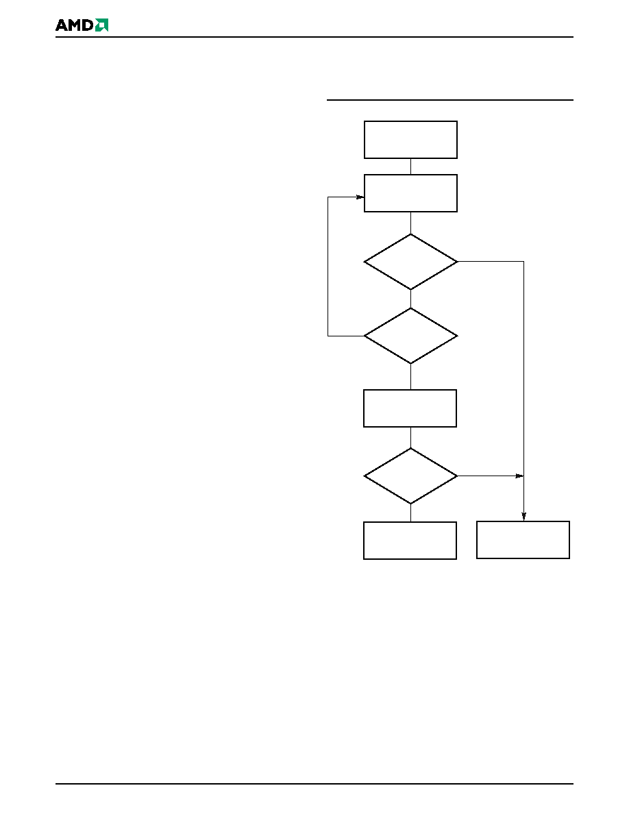
Figure 4 shows the Data# Polling algorithm.
DQ7 = Data?
Yes
No
DQ5 = 1?
No
Yes
FAIL
PASS
Read DQ7–DQ0
Addr = VA
Read DQ7–DQ0
Addr = VA
DQ7 = Data?
START
Notes:
1. VA = Valid address for programming. During a sector
erase operation, a valid address is an address within any
sector selected for erasure. During chip erase, a valid
address is any non-protected sector address.
2. DQ7 should be rechecked even if DQ5 = “1” because
DQ7 may change simultaneously with DQ5.
Figure 4.
Data# Polling Algorithm
相关PDF资料 |
PDF描述 |
|---|---|
| AM29F400BB-55ED | Flash Memory IC; Leaded Process Compatible:Yes; Memory Size:4Mbit; Package/Case:48-TSOP; Peak Reflow Compatible (260 C):Yes; Supply Voltage Max:5V; Access Time, Tacc:55ns; Series:AM29 RoHS Compliant: Yes |
| AM29F400BB-55SD | Flash Memory IC; Leaded Process Compatible:Yes; Memory Size:4Mbit; Package/Case:44-SOIC; Peak Reflow Compatible (260 C):Yes; Supply Voltage Max:5V; Access Time, Tacc:55ns; Series:AM29 RoHS Compliant: Yes |
| AM29F400BB-70ED | Flash Memory IC; Memory Size:4Mbit; Memory Configuration:256K x 16 / 512K x 8; Package/Case:48-TSOP; Leaded Process Compatible:Yes; Peak Reflow Compatible (260 C):Yes; Supply Voltage Max:5V; Access Time, Tacc:70ns RoHS Compliant: Yes |
| AM29F400BB-70SD | Flash Memory IC; Memory Size:4Mbit; Package/Case:44-SOIC; Leaded Process Compatible:Yes; Peak Reflow Compatible (260 C):Yes; Supply Voltage Max:5V; Access Time, Tacc:70ns; Series:AM29 RoHS Compliant: Yes |
| AM29F400BB-90EC | Flash Memory IC; Access Time, Tacc:90ns; Package/Case:48-TSOP; Leaded Process Compatible:No; Memory Configuration:256K x 16 / 512K x 8; Memory Size:4Mbit; Peak Reflow Compatible (260 C):No; Supply Voltage Max:5.5V RoHS Compliant: No |
相关代理商/技术参数 |
参数描述 |
|---|---|
| AM29F400BB120SI | 制造商:AMD 功能描述:* |
| AM29F400BB45EF | 制造商:Spansion 功能描述:NOR Flash Parallel 5V 4Mbit 512K/256K x 8bit/16bit 45ns 48-Pin TSOP |
| AM29F400BB-45EFT | 制造商:Spansion 功能描述: |
| AM29F400BB-45EI | 制造商:Spansion 功能描述: |
| AM29F400BB-45EI\\T | 制造商:Spansion 功能描述: |
发布紧急采购,3分钟左右您将得到回复。