- 您现在的位置:买卖IC网 > PDF目录366440 > AM29F800B-70SI (ADVANCED MICRO DEVICES INC) 8 Megabit (1,048,576 x 8-Bit/524,288 x 16-Bit) CMOS 5.0 Volt-only, Sector Erase Flash Memory PDF资料下载
参数资料
| 型号: | AM29F800B-70SI |
| 厂商: | ADVANCED MICRO DEVICES INC |
| 元件分类: | PROM |
| 英文描述: | 8 Megabit (1,048,576 x 8-Bit/524,288 x 16-Bit) CMOS 5.0 Volt-only, Sector Erase Flash Memory |
| 中文描述: | 512K X 16 FLASH 5V PROM, 70 ns, PDSO44 |
| 封装: | SOP-44 |
| 文件页数: | 16/41页 |
| 文件大小: | 267K |
| 代理商: | AM29F800B-70SI |
第1页第2页第3页第4页第5页第6页第7页第8页第9页第10页第11页第12页第13页第14页第15页当前第16页第17页第18页第19页第20页第21页第22页第23页第24页第25页第26页第27页第28页第29页第30页第31页第32页第33页第34页第35页第36页第37页第38页第39页第40页第41页
16
Am29F800T/Am29F800B
8/18/97
P R E L I M I N A R Y
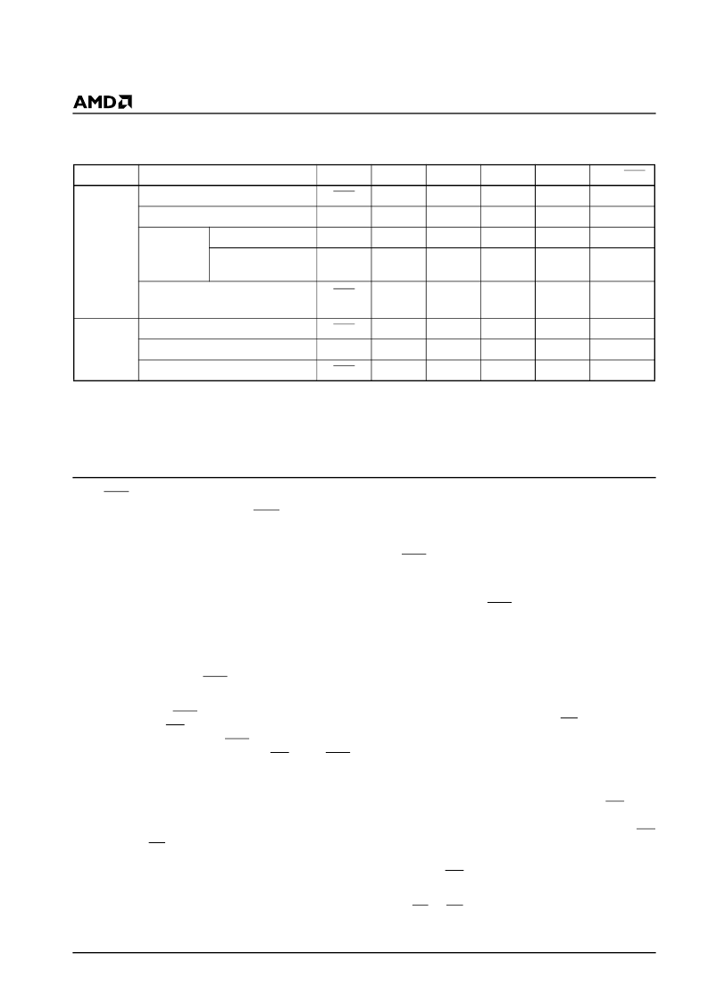
Write Operation Status
Table 8.
Hardware Sequence Flags
Notes:
1. DQ2 can be toggled when sector address applied is that of an erasing sector. Conversely, DQ2 cannot be toggled when the
sector address applied is that of a non-erasing sector. DQ2 is therefore used to determine which sectors are erasing and
which are not.
2. These status flags apply when outputs are read from the address of a non-erase-suspended sector.
3. If DQ5 is high (exceeded timing limits), successive reads from a problem sector will cause DQ2 to toggle.
DQ7: Data
Polling
The Am29F800 device features Data Polling as a
method to indicate to the host that the embedded algo-
rithms are in progress or completed. During the Em-
bedded Program Algorithm, an attempt to read the
device will produce the complement of the data last
written to DQ7. Upon completion of the Embedded Pro-
gram Algorithm, an attempt to read the device will pro-
duce the true data last written to DQ7. During the
Embedded Erase Algorithm, an attempt to read the de-
vice will produce a “0” at the DQ7 output.
Upon completion of the Embedded Erase Algorithm an
attempt to read the device will produce a “1” at the DQ7
output. The flowchart for Data Polling (DQ7) is shown
in Figure 3.
For chip erase, the Data Polling is valid after the rising
edge of the sixth WE pulse in the six write pulse se-
quence. For sector erase, the Data Polling is valid after
the last rising edge of the sector erase WE pulse. Data
Polling must be performed at sector addresses within
any of the sectors being erased and
not
a protected
sector. Otherwise, the status may not be valid.
Just prior to the completion of Embedded Algorithm op-
erations DQ7 may change asynchronously while the
output enable (OE) is asserted low. This means that the
device is driving status information on DQ7 at
one instant of time and then that byte’s valid data at the
next instant of time. Depending on when the
system samples the DQ7 output, it may read the status
or valid data. Even if the device has completed
the Embedded Algorithm operations and DQ7 has a
valid data, the data outputs on DQ0–DQ6 may be still
invalid. The valid data on DQ0–DQ7 will be read on the
successive read attempts.
The Data Polling feature is only active during the Em-
bedded Programming Algorithm, Embedded Erase Al-
gorithm, or sector erase time-out (see Table 7).
See Figure 11 for the Data Polling timing specifications
and diagrams.
DQ6: Toggle Bit
The Am29F800 also features the “Toggle Bit” as a
method to indicate to the host system that the embed-
ded algorithms are in progress or completed.
During an Embedded Program or Erase Algorithm cy-
cle, successive attempts to read (OE toggling) data
from the device at any address will result in DQ6 tog-
gling between one and zero. Once the Embedded Pro-
gram or Erase Algorithm cycle is completed, DQ6 will
stop toggling and valid data will be read on the next
successive attempt. During programming, the Toggle
Bit is valid after the rising edge of the fourth WE pulse
in the four write pulse sequence. For chip erase, the
Toggle Bit is valid after the rising edge of the sixth WE
pulse in the six write pulse sequence. For Sector erase,
the Toggle Bit is valid after the last rising edge of the
sector erase WE pulse. The Toggle Bit is active during
the sector erase time-out.
Either CE or OE toggling will cause DQ6 to toggle. In
addition, an Erase Suspend/Resume command will
Status
DQ7
DQ6
DQ5
DQ3
DQ2
RDY/BSY
In Progress
Byte Programming
DQ7
Toggle
0
0
No Tog
0
Program/Erase in Auto-Erase
0
Toggle
0
1
(Note 1)
0
Erase
suspend
mode
Erase sector address
1
No Tog
0
1
Toggle
1
Non-erase sector
address
Data
Data
Data
Data
Data
1
Program in erase suspend
DQ7
(Note 2)
Toggle
0
1
1
(Note 1)
0
Exceeded
Time
Limits
Byte Programming
DQ7
Toggle
1
0
No Tog
0
Program/Erase in Auto-Erase
0
Toggle
1
1
(Note 3)
0
Program in erase suspend
DQ7
Toggle
1
1
(Note 3)
0
相关PDF资料 |
PDF描述 |
|---|---|
| AM29F800B-70SIB | 8 Megabit (1,048,576 x 8-Bit/524,288 x 16-Bit) CMOS 5.0 Volt-only, Sector Erase Flash Memory |
| AM29F800B-90 | 8 Megabit (1,048,576 x 8-Bit/524,288 x 16-Bit) CMOS 5.0 Volt-only, Sector Erase Flash Memory |
| AM29F800B-90EC | 8 Megabit (1,048,576 x 8-Bit/524,288 x 16-Bit) CMOS 5.0 Volt-only, Sector Erase Flash Memory |
| AM29F800B-90ECB | 8 Megabit (1,048,576 x 8-Bit/524,288 x 16-Bit) CMOS 5.0 Volt-only, Sector Erase Flash Memory |
| AM29F800B-90EE | 8 Megabit (1,048,576 x 8-Bit/524,288 x 16-Bit) CMOS 5.0 Volt-only, Sector Erase Flash Memory |
相关代理商/技术参数 |
参数描述 |
|---|---|
| AM29F800BB-120DPC1 | 制造商:Spansion 功能描述:5V 8M FLASH KNOWN GOOD DIE W/BOTTOM BOOT (COMMERCIAL TEMP) - Gel-pak, waffle pack, wafer, diced wafer on film |
| AM29F800BB120SC | 制造商:Advanced Micro Devices 功能描述: |
| AM29F800BB-55EC | 制造商:Spansion 功能描述:NOR Flash Parallel 5V 8Mbit 1M/512K x 8bit/16bit 55ns 48-Pin TSOP |
| AM29F800BB-55EF | 功能描述:闪存 8M (1MX8/512KX16) Parallel NOR Fl 5V RoHS:否 制造商:ON Semiconductor 数据总线宽度:1 bit 存储类型:Flash 存储容量:2 MB 结构:256 K x 8 定时类型: 接口类型:SPI 访问时间: 电源电压-最大:3.6 V 电源电压-最小:2.3 V 最大工作电流:15 mA 工作温度:- 40 C to + 85 C 安装风格:SMD/SMT 封装 / 箱体: 封装:Reel |
| AM29F800BB-55EF\\T | 制造商:Spansion 功能描述:IC 8MEG(512K16)BOTTOM SCTOR 100K (CS39S) |
发布紧急采购,3分钟左右您将得到回复。