- 您现在的位置:买卖IC网 > PDF目录298821 > AM29LV200BT-70RSC (ADVANCED MICRO DEVICES INC) 256K X 8 FLASH 3V PROM, 70 ns, PDSO44 PDF资料下载
参数资料
| 型号: | AM29LV200BT-70RSC |
| 厂商: | ADVANCED MICRO DEVICES INC |
| 元件分类: | PROM |
| 英文描述: | 256K X 8 FLASH 3V PROM, 70 ns, PDSO44 |
| 封装: | MO-180AA, SOP-44 |
| 文件页数: | 39/41页 |
| 文件大小: | 843K |
| 代理商: | AM29LV200BT-70RSC |
第1页第2页第3页第4页第5页第6页第7页第8页第9页第10页第11页第12页第13页第14页第15页第16页第17页第18页第19页第20页第21页第22页第23页第24页第25页第26页第27页第28页第29页第30页第31页第32页第33页第34页第35页第36页第37页第38页当前第39页第40页第41页
Am29LV200B
7
DEVICE BUS OPERATIONS
This section describes the requirements and use of the
device bus operations, which are initiated through the
internal command register. The command register itself
does not occupy any addressable memory location.
The register is composed of latches that store the com-
mands, along with the address and data information
needed to execute the command. The contents of the
register serve as inputs to the internal state machine.
The state machine outputs dictate the function of the
device. Table 1 lists the device bus operations, the
inputs and control levels they require, and the resulting
output. The following subsections describe each of
these operations in further detail.
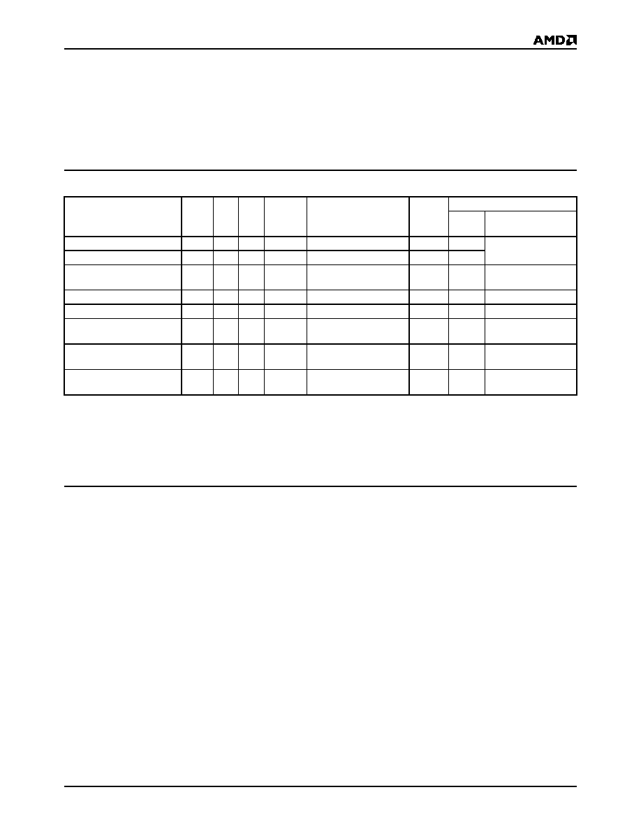
Table 1.
Am29LV200B Device Bus Operations
Legend:
L = Logic Low = VIL, H = Logic High = VIH, VID = 12.0 ± 0.5 V, X = Don’t Care, AIN = Addresses In, DIN = Data In, DOUT = Data Out
Notes:
1. Addresses are A16:A0 in word mode (BYTE# = VIH), A16:A-1 in byte mode (BYTE# = VIL).
2.
The sector protect and sector unprotect functions may also be implemented via programming equipment. See the “Sector
Protection/Unprotection” section.
Word/Byte Configuration
The BYTE# pin controls whether the device data I/O
pins DQ15–DQ0 operate in the byte or word configura-
tion. If the BYTE# pin is set at logic ‘1’, the device is in
word configuration, DQ15–DQ0 are active and con-
trolled by CE# and OE#.
If the BYTE# pin is set at logic ‘0’, the device is in byte
configuration, and only data I/O pins DQ0–DQ7 are
active and controlled by CE# and OE#. The data I/O
pins DQ8–DQ14 are tri-stated, and the DQ15 pin is
used as an input for the LSB (A-1) address function.
Requirements for Reading Array Data
To read array data from the outputs, the system must
drive the CE# and OE# pins to VIL. CE# is the power
control and selects the device. OE# is the output
control and gates array data to the output pins. WE#
should remain at VIH. The BYTE# pin determines
whether the device outputs array data in words or
bytes.
The internal state machine is set for reading array data
upon device power-up, or after a hardware reset. This
ensures that no spurious alteration of the memory
content occurs during the power transition. No
command is necessary in this mode to obtain array
data. Standard microprocessor read cycles that assert
valid addresses on the device address inputs produce
valid data on the device data outputs. The device
remains enabled for read access until the command
register contents are altered.
See “Reading Array Data” for more information. Refer
to the AC Read Operations table for timing specifica-
tions and to Figure 13 for the timing diagram. ICC1 in
the DC Characteristics table represents the active
current specification for reading array data.
Writing Commands/Command Sequences
To write a command or command sequence (which
includes programming data to the device and erasing
Operation
CE#
OE# WE# RESET#
Addresses
(Note 1)
DQ0–
DQ7
DQ8–DQ15
BYTE#
= VIH
BYTE#
= VIL
Read
L
H
AIN
DOUT
DOUT DQ8–DQ14 = High-Z,
DQ15 = A-1
Write
L
H
L
H
AIN
DIN
Standby
VCC ±
0.3 V
XX
VCC ±
0.3 V
X
High-Z
Output Disable
L
H
X
High-Z
Reset
X
L
X
High-Z
Sector Protect (Note 2)
L
H
L
VID
Sector Address, A6 = L,
A1 = H, A0 = L
DIN
XX
Sector Unprotect (Note 2)
L
H
L
VID
Sector Address, A6 = H,
A1 = H, A0 = L
DIN
XX
Temporary Sector
Unprotect
XX
X
VID
AIN
DIN
High-Z
相关PDF资料 |
PDF描述 |
|---|---|
| AM29LV200BB-70RSI | 256K X 8 FLASH 3V PROM, 70 ns, PDSO44 |
| AM29LV320DB120EE | 2M X 16 FLASH 3V PROM, 120 ns, PDSO48 |
| AM29LV320DB120WME | 2M X 16 FLASH 3V PROM, 120 ns, PBGA48 |
| AM29LV640MH101EF | 4M X 16 FLASH 3V PROM, 100 ns, PDSO56 |
| AM2D-11G | ACTIVE DELAY LINE, TRUE OUTPUT, PDSO8 |
相关代理商/技术参数 |
参数描述 |
|---|---|
| AM29LV256MH120RPGI | 制造商:Spansion 功能描述:FLASH PARALLEL 3V/3.3V 256MBIT 32MX8/16MX16 120NS 64BGA - Trays |
| AM29LV256MH123RPGI | 制造商:Advanced Micro Devices 功能描述: |
| AM29LV256MH94REI | 制造商:Spansion 功能描述:256M (32MX8/16MX16) 3V REG, MIRRORBIT, TSOP56, IND - Trays |
| AM29LV320DB120EI | 制造商:Spansion 功能描述:Flash Mem Parallel 3V/3.3V 32M-Bit 4M x 8/2M x 16 120ns 48-Pin TSOP |
| AM29LV320DB120WMI | 制造商:Spansion 功能描述:Flash Mem Parallel 3V/3.3V 32M-Bit 4M x 8/2M x 16 120ns 48-Pin FBGA |
发布紧急采购,3分钟左右您将得到回复。