- 您现在的位置:买卖IC网 > PDF目录10533 > AMIS30663CANG2G (ON Semiconductor)TRANSCEIVER CAN HS 3.3V 8-SOIC PDF资料下载
参数资料
| 型号: | AMIS30663CANG2G |
| 厂商: | ON Semiconductor |
| 文件页数: | 2/11页 |
| 文件大小: | 0K |
| 描述: | TRANSCEIVER CAN HS 3.3V 8-SOIC |
| 标准包装: | 96 |
| 类型: | 收发器 |
| 驱动器/接收器数: | 1/1 |
| 规程: | CAN |
| 电源电压: | 4.75 V ~ 5.25 V |
| 安装类型: | 表面贴装 |
| 封装/外壳: | 8-SOIC(0.154",3.90mm 宽) |
| 供应商设备封装: | 8-SOICN |
| 包装: | 管件 |
| 产品目录页面: | 1115 (CN2011-ZH PDF) |
| 其它名称: | 766-1015 |
AMIS30663
http://onsemi.com
10
Soldering
Introduction to Soldering Surface Mount Packages
This text gives a very brief insight to a complex
technology. A more indepth account of soldering ICs can
be found in the ON Semiconductor “Data Handbook IC26;
Integrated Circuit Packages” (document order number 9398
652 90011). There is no soldering method that is ideal for all
surface mount IC packages. Wave soldering is not always
suitable for surface mount ICs, or for printedcircuit boards
(PCB) with high population densities. In these situations
reflow soldering is often used.
Reflow Soldering
Reflow soldering requires solder paste (a suspension of
fine solder particles, flux and binding agent) to be applied to
the PCB by screen printing, stencilling or pressuresyringe
dispensing before package placement. Several methods
exist for reflowing; for example, infrared/convection
heating in a conveyor type oven.
Throughput times (preheating, soldering and cooling)
vary between 100 and 200 seconds depending on heating
method. Typical reflow peak temperatures range from 215
to 250
°C. The topsurface temperature of the packages
should preferably be kept below 230
°C.
Wave Soldering
Conventional single wave soldering is not recommended
for surface mount devices (SMDs) or PCBs with a high
component density, as solder bridging and nonwetting can
present major problems. To overcome these problems the
doublewave soldering method was specifically developed.
If wave soldering is used the following conditions must be
observed for optimal results:
Use a doublewave soldering method comprising a
turbulent wave with high upward pressure followed by
a smooth laminar wave.
For packages with leads on two sides and a pitch (e):
1. Larger than or equal to 1.27 mm, the footprint
longitudinal axis is preferred to be parallel to the
transport direction of the PCB;
2. Smaller than 1.27 mm, the footprint longitudinal
axis must be parallel to the transport direction of
the PCB. The footprint must incorporate solder
thieves at the downstream end.
For packages with leads on four sides, the footprint
must be placed at a 45
° angle to the transport direction
of the PCB. The footprint must incorporate solder
thieves downstream and at the side corners.
During placement and before soldering, the package must
be fixed with a droplet of adhesive. The adhesive can be
applied by screen printing, pin transfer or syringe
dispensing. The package can be soldered after the adhesive
is cured. Typical dwell time is four seconds at 250
°C. A
mildlyactivated flux will eliminate the need for removal of
corrosive residues in most applications.
Manual Soldering
Fix the component by first soldering two diagonally
opposite end leads. Use a low voltage (24 V or less)
soldering iron applied to the flat part of the lead. Contact
time must be limited to 10 seconds at up to 300
°C.
When using a dedicated tool, all other leads can be
soldered in one operation within two to five seconds
between 270 and 320
°C.
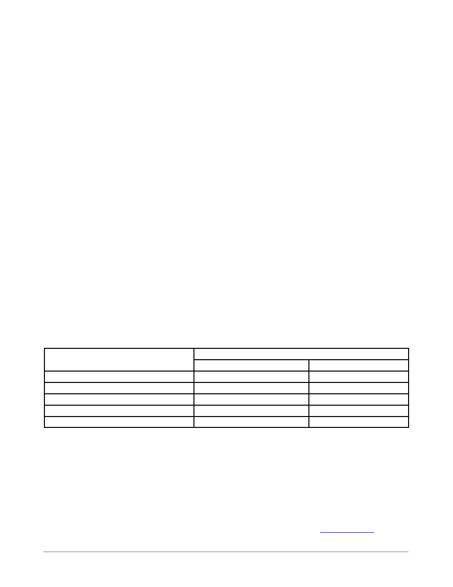
Table 9. Soldering Process
Package
Soldering Method
Wave
Reflow (Note 8)
BGA, SQFP
Not suitable
Suitable
HLQFP, HSQFP, HSOP, HTSSOP, SMS
Not suitable (Note 9)
Suitable
PLCC (Note 10), SO, SOJ
Suitable
LQFP, QFP, TQFP
Suitable
SSOP, TSSOP, VSO
Not recommended (Note 12)
Suitable
8. All surface mount (SMD) packages are moisture sensitive. Depending upon the moisture content, the maximum temperature (with respect
to time) and body size of the package, there is a risk that internal or external package cracks may occur due to vaporization of the moisture
in them (the so called popcorn effect). For details, refer to the drypack information in the “Data Handbook IC26; Integrated Circuit Packages;
Section: Packing Methods.”
9. These packages are not suitable for wave soldering as a solder joint between the PCB and heatsink (at bottom version) can not be achieved,
and as solder may stick to the heatsink (on top version).
10.If wave soldering is considered, then the package must be placed at a 45° angle to the solder wave direction. The package footprint must
incorporate solder thieves downstream and at the side corners.
11. Wave soldering is only suitable for LQFP, TQFP and QFP packages with a pitch (e) equal to or larger than 0.8 mm; it is definitely not suitable
for packages with a pitch (e) equal to or smaller than 0.65 mm.
12.Wave soldering is only suitable for SSOP and TSSOP packages with a pitch (e) equal to or larger than 0.65 mm; it is definitely not suitable
for packages with a pitch (e) equal to or smaller than 0.5 mm.
Company or Product Inquiries
For more information about ON Semiconductor’s products or services visit our Web site at http://onsemi.com.
相关PDF资料 |
PDF描述 |
|---|---|
| VI-B4T-MX-F2 | CONVERTER MOD DC/DC 6.5V 75W |
| EXP-0921/05/S | CONN RCPT 5POS IP68 W/SOCKETS |
| LTC1415CG#PBF | IC A/D CONV 12BIT SAMPLNG 28SSOP |
| AMIS30660CANH2G | TRANSCEIVER CAN HS 5V 8-SOIC |
| VE-J3Y-MY-F2 | CONVERTER MOD DC/DC 3.3V 33W |
相关代理商/技术参数 |
参数描述 |
|---|---|
| AMIS30663CANG2RG | 功能描述:CAN 接口集成电路 HS CAN TRANSC 3.3V RoHS:否 制造商:Texas Instruments 类型:Transceivers 工作电源电压:5 V 电源电流: 工作温度范围:- 40 C to + 85 C 封装 / 箱体:SOIC-8 封装:Tube |
| AMIS30663NGA | 制造商:AMI 制造商全称:AMI 功能描述:High Speed CAN Transceiver |
| AMIS-39100 | 制造商:ONSEMI 制造商全称:ON Semiconductor 功能描述:Octal High Side Driver with Protection |
| AMIS39100AGA | 制造商:AMI 制造商全称:AMI 功能描述:Octal High Side Driver with Protection |
| AMIS39100PNPB3G | 功能描述:功率驱动器IC OCTAL HS DRVR 12V RoHS:否 制造商:Micrel 产品:MOSFET Gate Drivers 类型:Low Cost High or Low Side MOSFET Driver 上升时间: 下降时间: 电源电压-最大:30 V 电源电压-最小:2.75 V 电源电流: 最大功率耗散: 最大工作温度:+ 85 C 安装风格:SMD/SMT 封装 / 箱体:SOIC-8 封装:Tube |
发布紧急采购,3分钟左右您将得到回复。