- 您现在的位置:买卖IC网 > PDF目录375330 > AO3422 (ALPHA) N-Channel Enhancement Mode Field Effect Transistor PDF资料下载
参数资料
| 型号: | AO3422 |
| 厂商: | ALPHA |
| 英文描述: | N-Channel Enhancement Mode Field Effect Transistor |
| 中文描述: | N沟道增强型场效应管 |
| 文件页数: | 2/4页 |
| 文件大小: | 139K |
| 代理商: | AO3422 |
AO3422
Symbol
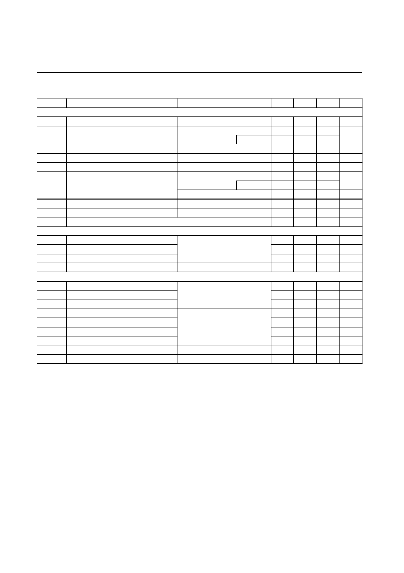
STATIC PARAMETERS
Drain-Source Breakdown Voltage
Min
Typ
Max
Units
BV
DSS
55
V
1
5
T
J
=55°C
I
GSS
V
GS(th)
I
D(ON)
±100
2
nA
V
A
0.6
10
1.3
125
175
157
11
0.78
160
210
200
T
J
=125°C
m
Ω
S
V
A
g
FS
V
SD
I
S
DYNAMIC PARAMETERS
Input Capacitance
Output Capacitance
1
1
C
iss
C
oss
C
rss
R
g
SWITCHING PARAMETERS
Total Gate Charge
Gate Source Charge
Gate Drain Charge
Turn-On DelayTime
Turn-On Rise Time
Turn-Off DelayTime
214
31
12.6
1.3
300
pF
pF
pF
Ω
3
Q
g
Q
gs
Q
gd
t
D(on)
t
r
t
D(off)
t
f
t
rr
Q
rr
2.6
0.6
0.8
2.3
2.4
16.5
2
20
17
3.3
nC
nC
nC
ns
ns
ns
ns
ns
nC
30
THIS PRODUCT HAS BEEN DESIGNED AND QUALIFIED FOR THE CONSUMER MARKET. APPLICATIONS OR USES AS CRITICAL
COMPONENTS IN LIFE SUPPORT DEVICES OR SYSTEMS ARE NOT AUTHORIZED. AOS DOES NOT ASSUME ANY LIABILITY ARISING
OUT OF SUCH APPLICATIONS OR USES OF ITS PRODUCTS. AOS RESERVES THE RIGHT TO IMPROVE PRODUCT DESIGN,
FUNCTIONS AND RELIABILITY WITHOUT NOTICE.
Body Diode Reverse Recovery Time
Body Diode Reverse Recovery Charge
Turn-Off Fall Time
V
GS
=4.5V, V
DS
=27.5V, I
D
=2.1A
V
GS
=10V, V
DS
=27.5V, R
L
=12
Ω
,
R
GEN
=3
Ω
Reverse Transfer Capacitance
Gate resistance
V
GS
=0V, V
DS
=0V, f=1MHz
Forward Transconductance
Diode Forward Voltage
Maximum Body-Diode Continuous Current
V
DS
=5V, I
D
=2.1A
I
S
=1A
V
GS
=0V, V
DS
=25V, f=1MHz
R
DS(ON)
Static Drain-Source On-Resistance
V
GS
=4.5V, I
D
=2.1A
m
Ω
V
GS
=2.5V, I
D
=1.5A
Gate Threshold Voltage
On state drain current
V
DS
=V
GS
I
D
=250
μ
A
V
GS
=4.5V, V
DS
=5V
V
DS
=44V, V
GS
=0V
μ
A
Gate-Source leakage current
V
DS
=0V, V
GS
=±12V
I
F
=2.1A, dI/dt=100A/
μ
s
I
F
=2.1A, dI/dt=100A/
μ
s
Electrical Characteristics (T
J
=25°C unless otherwise noted)
Parameter
Conditions
I
D
=10mA, V
GS
=0V
I
DSS
Zero Gate Voltage Drain Current
A: The value of R
θ
JA
is measured with the device mounted on 1in
2
FR-4 board with 2oz. Copper, in a still air environment with T
A
=25°C. The
value in any given application depends on the user's specific board design. The current rating is based on the t
≤
10s thermal resistance rating.
B: Repetitive rating, pulse width limited by junction temperature.
C. The R
θ
JA
is the sum of the thermal impedence from junction to lead R
θ
JL
and lead to ambient.
D. The static characteristics in Figures 1 to 6 are obtained using 80
μ
s pulses, duty cycle 0.5% max.
E. These tests are performed with the device mounted on 1 in
curve provides a single pulse rating.
Rev0: Oct 2005
2
FR-4 board with 2oz. Copper, in a still air environment with T
A
=25°C. The SOA
Alpha & Omega Semiconductor, Ltd.
相关PDF资料 |
PDF描述 |
|---|---|
| AO3422L | N-Channel Enhancement Mode Field Effect Transistor |
| AO3423 | P-Channel Enhancement Mode Field Effect Transistor |
| AO3424 | N-Channel Enhancement Mode Field Effect Transistor |
| AOD454 | N-Channel Enhancement Mode Field Effect Transistor |
| AOD454L | N-Channel Enhancement Mode Field Effect Transistor |
相关代理商/技术参数 |
参数描述 |
|---|---|
| AO3422_10 | 制造商:AOSMD 制造商全称:Alpha & Omega Semiconductors 功能描述:N-Channel Enhancement Mode Field Effect Transistor |
| AO3422L | 制造商:AOSMD 制造商全称:Alpha & Omega Semiconductors 功能描述:N-Channel Enhancement Mode Field Effect Transistor |
| AO3423 | 功能描述:MOSFET P-CH -20V -2A SOT23 RoHS:是 类别:分离式半导体产品 >> FET - 单 系列:- 标准包装:1,000 系列:MESH OVERLAY™ FET 型:MOSFET N 通道,金属氧化物 FET 特点:逻辑电平门 漏极至源极电压(Vdss):200V 电流 - 连续漏极(Id) @ 25° C:18A 开态Rds(最大)@ Id, Vgs @ 25° C:180 毫欧 @ 9A,10V Id 时的 Vgs(th)(最大):4V @ 250µA 闸电荷(Qg) @ Vgs:72nC @ 10V 输入电容 (Ciss) @ Vds:1560pF @ 25V 功率 - 最大:40W 安装类型:通孔 封装/外壳:TO-220-3 整包 供应商设备封装:TO-220FP 包装:管件 |
| AO3423_102 | 功能描述:MOSFET P-CH 20V SOT23 制造商:alpha & omega semiconductor inc. 系列:- 包装:带卷(TR) 零件状态:最後搶購 安装类型:表面贴装 供应商器件封装:SOT-23 封装/外壳:TO-236-3,SC-59,SOT-23-3 标准包装:3,000 |
| AO3423_11 | 制造商:AOSMD 制造商全称:Alpha & Omega Semiconductors 功能描述:20V P-Channel MOSFET |
发布紧急采购,3分钟左右您将得到回复。