参数资料
| 型号: | APA075-PQ208A |
| 厂商: | Microsemi SoC |
| 文件页数: | 140/178页 |
| 文件大小: | 0K |
| 描述: | IC FPGA PROASIC+ 75K 208-PQFP |
| 标准包装: | 24 |
| 系列: | ProASICPLUS |
| RAM 位总计: | 27648 |
| 输入/输出数: | 158 |
| 门数: | 75000 |
| 电源电压: | 2.375 V ~ 2.625 V |
| 安装类型: | 表面贴装 |
| 工作温度: | -40°C ~ 125°C |
| 封装/外壳: | 208-BFQFP |
| 供应商设备封装: | 208-PQFP(28x28) |
第1页第2页第3页第4页第5页第6页第7页第8页第9页第10页第11页第12页第13页第14页第15页第16页第17页第18页第19页第20页第21页第22页第23页第24页第25页第26页第27页第28页第29页第30页第31页第32页第33页第34页第35页第36页第37页第38页第39页第40页第41页第42页第43页第44页第45页第46页第47页第48页第49页第50页第51页第52页第53页第54页第55页第56页第57页第58页第59页第60页第61页第62页第63页第64页第65页第66页第67页第68页第69页第70页第71页第72页第73页第74页第75页第76页第77页第78页第79页第80页第81页第82页第83页第84页第85页第86页第87页第88页第89页第90页第91页第92页第93页第94页第95页第96页第97页第98页第99页第100页第101页第102页第103页第104页第105页第106页第107页第108页第109页第110页第111页第112页第113页第114页第115页第116页第117页第118页第119页第120页第121页第122页第123页第124页第125页第126页第127页第128页第129页第130页第131页第132页第133页第134页第135页第136页第137页第138页第139页当前第140页第141页第142页第143页第144页第145页第146页第147页第148页第149页第150页第151页第152页第153页第154页第155页第156页第157页第158页第159页第160页第161页第162页第163页第164页第165页第166页第167页第168页第169页第170页第171页第172页第173页第174页第175页第176页第177页第178页
ProASICPLUS Flash Family FPGAs
2- 54
v5.9
Embedded Memory Specifications
This section discusses ProASICPLUS SRAM/FIFO embedded
memory and its interface signals, including timing
diagrams that show the relationships of signals as they
pertain to single embedded memory blocks (Table 2-51).
Table 2-13 on page 2-21 shows basic SRAM and FIFO
configurations. Simultaneous read and write to the same
location must be done with care. On such accesses the DI
bus is output to the DO bus. Refer to the ProASICPLUS
RAM and FIFO Blocks application note for more
information.
Enclosed Timing Diagrams—SRAM Mode:
Embedded Memory Specifications
The difference between synchronous transparent and
pipeline modes is the timing of all the output signals
from the memory. In transparent mode, the outputs will
change within the same clock cycle to reflect the data
requested by the currently valid access to the memory. If
clock cycles are short (high clock speed), the data
requires most of the clock cycle to change to valid values
(stable signals). Processing of this data in the same clock
cycle is nearly impossible. Most designers add registers at
all outputs of the memory to push the data processing
into the next clock cycle. An entire clock cycle can then
be used to process the data. To simplify use of this
memory
setup,
suitable
registers
have
been
implemented as part of the memory primitive and are
available to the user in the synchronous pipeline mode.
In this mode, the output signals will change shortly after
the second rising edge, following the initiation of the
read access.
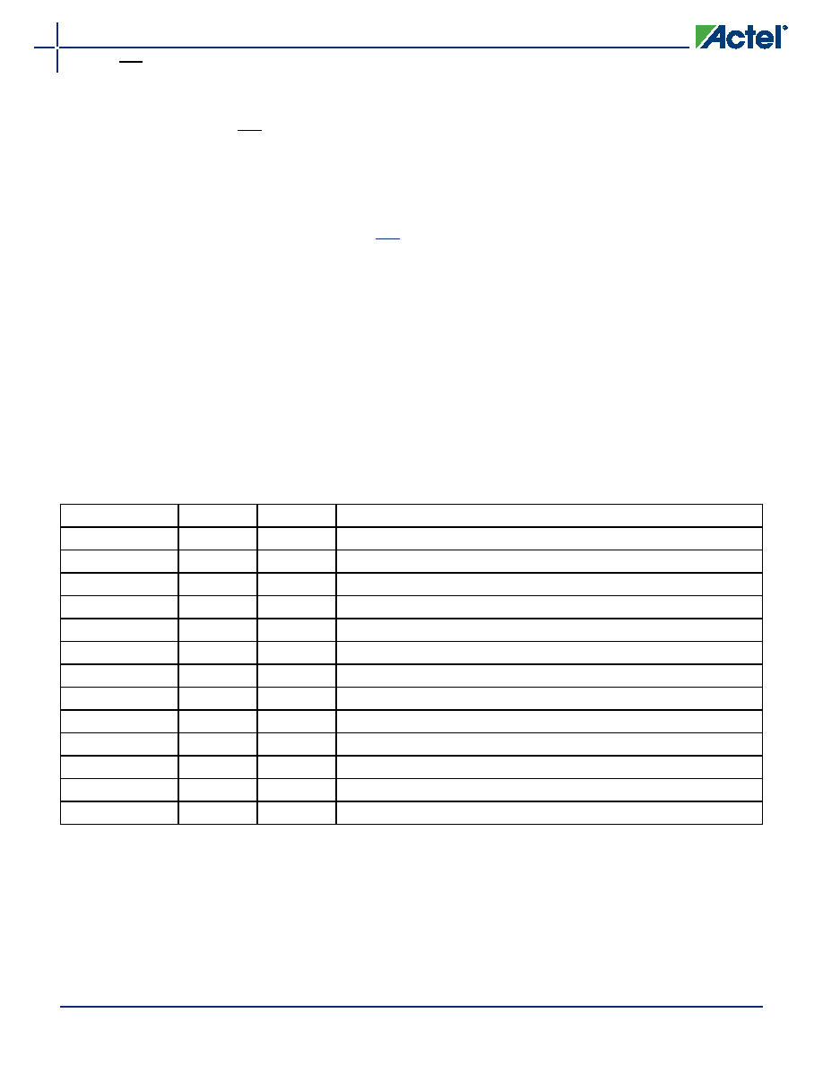
Table 2-51 Memory Block SRAM Interface Signals
SRAM Signal
Bits
In/Out
Description
WCLKS
1
In
Write clock used on synchronization on write side
RCLKS
1
In
Read clock used on synchronization on read side
RADDR[0:7]
8
In
Read address
RBLKB
1
In
True read block select (active Low)
RDB
1
In
True read pulse (active Low)
WADDR[0:7]
8
In
Write address
WBLKB
1
In
Write block select (active Low)
DI[0:8]
9
In
Input data bits [0:8], [8] can be used for parity In
WRB
1
In
Negative true write pulse
DO[0:8]
9
Out
Output data bits [0:8], [8] can be used for parity Out
RPE
1
Out
Read parity error (active High)
WPE
1
Out
Write parity error (active High)
PARODD
1
In
Selects odd parity generation/detect when high, even when low
Note: Not all signals shown are used in all modes.
相关PDF资料 |
PDF描述 |
|---|---|
| ASM31DTAD-S189 | CONN EDGECARD 62POS R/A .156 SLD |
| APA075-PQG208A | IC FPGA PROASIC+ 75K 208-PQFP |
| APA150-FG256 | IC FPGA PROASIC+ 150K 256-FBGA |
| APA150-FGG256 | IC FPGA PROASIC+ 150K 256-FBGA |
| A3P125-1FGG144T | IC FPGA 1KB FLASH 125K 144-FBGA |
相关代理商/技术参数 |
参数描述 |
|---|---|
| APA075-PQ208I | 功能描述:IC FPGA PROASIC+ 75K 208-PQFP RoHS:否 类别:集成电路 (IC) >> 嵌入式 - FPGA(现场可编程门阵列) 系列:ProASICPLUS 标准包装:90 系列:ProASIC3 LAB/CLB数:- 逻辑元件/单元数:- RAM 位总计:36864 输入/输出数:157 门数:250000 电源电压:1.425 V ~ 1.575 V 安装类型:表面贴装 工作温度:-40°C ~ 125°C 封装/外壳:256-LBGA 供应商设备封装:256-FPBGA(17x17) |
| APA075-PQ896A | 制造商:ACTEL 制造商全称:Actel Corporation 功能描述:Automotive-Grade ProASIC Flash Family FPGAs |
| APA075-PQB | 制造商:ACTEL 制造商全称:Actel Corporation 功能描述:ProASIC Flash Family FPGAs |
| APA075-PQES | 制造商:ACTEL 制造商全称:Actel Corporation 功能描述:ProASIC Flash Family FPGAs |
| APA075-PQG208 | 功能描述:IC FPGA PROASIC+ 75K 208-PQFP RoHS:是 类别:集成电路 (IC) >> 嵌入式 - FPGA(现场可编程门阵列) 系列:ProASICPLUS 标准包装:90 系列:ProASIC3 LAB/CLB数:- 逻辑元件/单元数:- RAM 位总计:36864 输入/输出数:157 门数:250000 电源电压:1.425 V ~ 1.575 V 安装类型:表面贴装 工作温度:-40°C ~ 125°C 封装/外壳:256-LBGA 供应商设备封装:256-FPBGA(17x17) |
发布紧急采购,3分钟左右您将得到回复。