- 您现在的位置:买卖IC网 > PDF目录369364 > APT1201R4SLL (Advanced Power Technology Ltd.) Power MOS 7TM is a new generation of low loss, high voltage, N-Channel enhancement mode power MOSFETS. PDF资料下载
参数资料
| 型号: | APT1201R4SLL |
| 厂商: | Advanced Power Technology Ltd. |
| 英文描述: | Power MOS 7TM is a new generation of low loss, high voltage, N-Channel enhancement mode power MOSFETS. |
| 中文描述: | 电源MOS 7TM是一个低损耗,高电压,N沟道增强型功率MOSFET的新一代。 |
| 文件页数: | 2/2页 |
| 文件大小: | 69K |
| 代理商: | APT1201R4SLL |
DYNAMIC CHARACTERISTICS
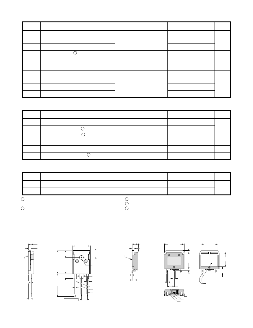
APT1201R4 BLL - SLL
0
15.49 (.610)
5.38 (.212)
6.15 (.242) BSC
4.50 (.177) Max.
19.81 (.780)
20.80 (.819)
1.65 (.065)
1.01 (.040)
3.50 (.138)
2.87 (.113)
4.69 (.185)
1.49 (.059)
2.21 (.087)
0.40 (.016)
D
Drain
Source
Gate
5.45 (.215) BSC
2-Plcs.
Dimensions in Millimeters and (Inches)
TO
-
247 Package Outline
15.95 (.628)
1.22 (.048)
5.45 (.215) BSC
4.98 (.196)
1.47 (.058)
2.67 (.105)
{3 Plcs}
0.46 (.018)
0.020 (.001)
Dimensions in Millimeters (Inches)
Heat Sink (Drain)
3.81 (.150)
D
(
1.98 (.078)
Gate
Drain
Source
1.27 (.050)
11.51 (.453)
13.41 (.528)
Revised
1.04 (.041)
13.79 (.543)
4/18/95
D
3
PAK Package Outline
APT's devices are covered by one or more of the following U.S.patents:
4,895,810
5,256,583
5,045,903
4,748,103
5,089,434
5,283,202
5,182,234
5,231,474
5,019,522
5,434,095
5,262,336
5,528,058
Reverse Recovery Time (I
S
= -I
D[Cont.]
, dl
S
/dt = 100A/μs)
Reverse Recovery Charge (I
S
= -I
D[Cont.]
, dl
S
/dt = 100A/μs)
Peak Diode Recovery
dv
/
dt 5
INFORMATION
Symbol
C
iss
C
oss
C
rss
Q
g
Q
gs
Q
gd
t
d(on)
t
r
t
d(off)
t
f
Test Conditions
V
GS
= 0V
V
DS
= 25V
f = 1 MHz
GS
= 10V
DD
= 0.5 V
DSS
= I
D[Cont.]
@ 25°C
GS
= 15V
DD
= 0.5 V
DSS
= I
D[Cont.]
@ 25°C
R
G
= 1.6
W
MIN
TYP
MAX
2300
320
241
81
10
48
14
9
44
23
UNIT
pF
nC
ns
Characteristic
Input Capacitance
Output Capacitance
Reverse Transfer Capacitance
Total Gate Charge
3
Gate-Source Charge
Gate-Drain ("Miller") Charge
Turn-on Delay Time
Rise Time
Turn-off Delay Time
Fall Time
Characteristic / Test Conditions
Continuous Source Current (Body Diode)
Pulsed Source Current
1
(Body Diode)
Diode Forward Voltage
2
(V
GS
= 0V, I
S
= -I
D[Cont.]
)
SOURCE-DRAIN DIODE RATINGS AND CHARACTERISTICS
UNIT
Amps
Volts
ns
μC
V/ns
MIN
TYP
MAX
9
36
1.3
500
7.0
10
1
Repetitive Rating: Pulse width limited by maximum junction
temperature.
2
Pulse Test: Pulse width < 380 μs, Duty Cycle < 2%
3
See MIL-STD-750 Method 3471
4
Starting T
j
=
+25°C, L = 29.9mH, R
G
=
25
W
, Peak I
L
= 9A
5 dv
/
dt
numbers reflect the limitations of the test circuit rather than the
device itself.
I
S
£
-
I
D
[
Cont.
]
di
/
dt
£
700A/μs
V
R
£
V
DSS
T
J
£
150
°
C
APT Reserves the right to change, without notice, the specifications and information contained herein.
THERMAL CHARACTERISTICS
Symbol
R
q
JC
R
q
JA
MIN
TYP
MAX
0.42
40
UNIT
°C/W
Characteristic
Junction to Case
Junction to Ambient
Symbol
I
S
I
SM
V
SD
t
rr
Q
rr
dv
/
dt
相关PDF资料 |
PDF描述 |
|---|---|
| APT12031JLL | Power MOS 7TM is a new generation of low loss, high voltage, N-Channel enhancement mode power MOSFETS. |
| APT12067B2LL | Power MOS 7TM is a new generation of low loss, high voltage, N-Channel enhancement mode power MOSFETS |
| APT12GT60BR | The Thunderbolt IGBT⑩ is a new generation of high voltage power IGBTs |
| APT12GT60KR | The Thunderbolt IGBT⑩ is a new generation of high voltage power IGBTs. |
| APT20GF120BR | The Fast IGBT is a new generation of high voltage power IGBTs. |
相关代理商/技术参数 |
参数描述 |
|---|---|
| APT1201R5BVFR | 制造商:ADPOW 制造商全称:Advanced Power Technology 功能描述:POWER MOS V |
| APT1201R5BVFRG | 功能描述:MOSFET N-CH 1200V 10A TO-247 RoHS:是 类别:分离式半导体产品 >> FET - 单 系列:POWER MOS V® 标准包装:1,000 系列:MESH OVERLAY™ FET 型:MOSFET N 通道,金属氧化物 FET 特点:逻辑电平门 漏极至源极电压(Vdss):200V 电流 - 连续漏极(Id) @ 25° C:18A 开态Rds(最大)@ Id, Vgs @ 25° C:180 毫欧 @ 9A,10V Id 时的 Vgs(th)(最大):4V @ 250µA 闸电荷(Qg) @ Vgs:72nC @ 10V 输入电容 (Ciss) @ Vds:1560pF @ 25V 功率 - 最大:40W 安装类型:通孔 封装/外壳:TO-220-3 整包 供应商设备封装:TO-220FP 包装:管件 |
| APT1201R5BVR | 制造商:ADPOW 制造商全称:Advanced Power Technology 功能描述:Power MOS V is a new generation of high voltage N-Channel enhancement mode power MOSFETs. |
| APT1201R5BVRG | 制造商:Microsemi Corporation 功能描述:POWER MOSFET TRANSISTOR 制造商:Microsemi 功能描述:POWER MOSFET TRANSISTOR |
| APT1201R5SVFR | 制造商:ADPOW 制造商全称:Advanced Power Technology 功能描述:POWER MOS V |
发布紧急采购,3分钟左右您将得到回复。