- 您现在的位置:买卖IC网 > PDF目录57947 > APT44H60J (MICROSEMI POWER PRODUCTS GROUP) 44 A, 600 V, 0.11 ohm, N-CHANNEL, Si, POWER, MOSFET PDF资料下载
参数资料
| 型号: | APT44H60J |
| 厂商: | MICROSEMI POWER PRODUCTS GROUP |
| 元件分类: | JFETs |
| 英文描述: | 44 A, 600 V, 0.11 ohm, N-CHANNEL, Si, POWER, MOSFET |
| 封装: | ROHS COMPLIANT, ISOTOP-4 |
| 文件页数: | 2/4页 |
| 文件大小: | 273K |
| 代理商: | APT44H60J |
Static Characteristics
TJ = 25°C unless otherwise specied
Source-Drain Diode Characteristics
Dynamic Characteristics
TJ = 25°C unless otherwise specied
1 Repetitive Rating: Pulse width and case temperature limited by maximum junction temperature.
2 Starting at T
J = 25°C, L = 3.39mH, RG = 2.2, IAS = 33A.
3 Pulse test: Pulse Width < 380s, duty cycle < 2%.
4 C
o(cr) is dened as a xed capacitance with the same stored charge as COSS with VDS = 67% of V(BR)DSS.
5 C
o(er) is dened as a xed capacitance with the same stored energy as COSS with VDS = 67% of V(BR)DSS. To calculate Co(er) for any value of
V
DS less than V(BR)DSS, use this equation: Co(er) = -1.28E-7/VDS^2 + 5.36E-8/VDS + 2.00E-10.
6 R
G is external gate resistance, not including internal gate resistance or gate driver impedance. (MIC4452)
Microsemi reserves the right to change, without notice, the specications and information contained herein.
G
D
S
Unit
V
V/°C
V
mV/°C
A
nA
Unit
S
pF
nC
ns
Unit
A
V
ns
C
A
V/ns
Min
Typ
Max
600
0.57
0.091
0.11
3
4
5
-10
100
1000
±100
Min
Typ
Max
65
13190
135
1210
645
335
330
70
140
75
85
225
70
Min
Typ
Max
44
245
1.0
250
460
1.27
3.32
9.1
13.5
30
Test Conditions
V
GS = 0V, ID = 250A
Reference to 25°C, I
D = 250A
V
GS = 10V, ID = 33A
V
GS = VDS, ID = 2.5mA
V
DS = 600V
T
J = 25°C
V
GS = 0V
T
J = 125°C
V
GS = ±30V
Test Conditions
V
DS = 50V, ID = 33A
V
GS = 0V, VDS = 25V
f = 1MHz
V
GS = 0V, VDS = 0V to 400V
V
GS = 0 to 10V, ID = 33A,
V
DS = 300V
Resistive Switching
V
DD = 400V, ID = 33A
R
G = 2.2
6
, V
GG = 15V
Test Conditions
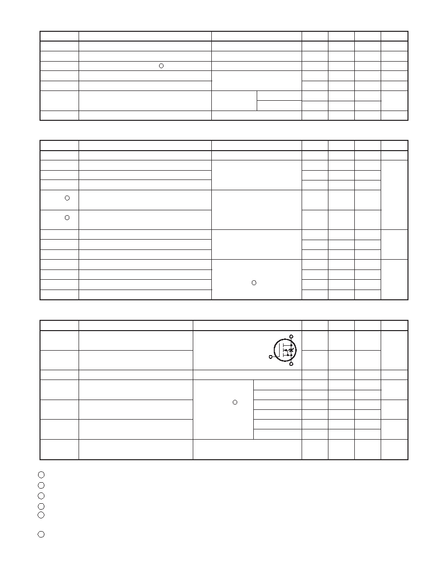
MOSFET symbol
showing the
integral reverse p-n
junction diode
(body diode)
I
SD = 33A, TJ = 25°C, VGS = 0V
T
J = 25°C
T
J = 125°C
I
SD = 33A
3
T
J = 25°C
di
SD/dt = 100A/s
T
J = 125°C
V
DD = 100V
T
J = 25°C
T
J = 125°C
I
SD ≤ 33A, di/dt ≤1000A/s, VDD = 400V,
T
J = 125°C
Parameter
Drain-Source Breakdown Voltage
Breakdown Voltage Temperature Coefcient
Drain-Source On Resistance 3
Gate-Source Threshold Voltage
Threshold Voltage Temperature Coefcient
Zero Gate Voltage Drain Current
Gate-Source Leakage Current
Parameter
Forward Transconductance
Input Capacitance
Reverse Transfer Capacitance
Output Capacitance
Effective Output Capacitance, Charge Related
Effective Output Capacitance, Energy Related
Total Gate Charge
Gate-Source Charge
Gate-Drain Charge
Turn-On Delay Time
Current Rise Time
Turn-Off Delay Time
Current Fall Time
Parameter
Continuous Source Current
(Body Diode)
Pulsed Source Current
(Body Diode) 1
Diode Forward Voltage
Reverse Recovery Time
Reverse Recovery Charge
Reverse Recovery Current
Peak Recovery dv/dt
Symbol
V
BR(DSS)
V
BR(DSS)/TJ
R
DS(on)
V
GS(th)
V
GS(th)/TJ
I
DSS
I
GSS
Symbol
g
fs
C
iss
C
rss
C
oss
C
o(cr)
4
C
o(er)
5
Q
g
Q
gs
Q
gd
t
d(on)
t
r
t
d(off)
t
f
Symbol
I
S
I
SM
V
SD
t
rr
Q
rr
I
rrm
dv/dt
050-8147
Rev
A
6-2007
APT44H60J
相关PDF资料 |
PDF描述 |
|---|---|
| APT45GP120JDQ2 | 75 A, 1200 V, N-CHANNEL IGBT |
| APT45GP120JDQ2 | 75 A, 1200 V, N-CHANNEL IGBT |
| APT5010B2FLC | 47 A, 500 V, 0.1 ohm, N-CHANNEL, Si, POWER, MOSFET |
| APT5010JFLC | 44 A, 500 V, 0.1 ohm, N-CHANNEL, Si, POWER, MOSFET |
| APT5010JFLL | 41 A, 500 V, 0.1 ohm, N-CHANNEL, Si, POWER, MOSFET |
相关代理商/技术参数 |
参数描述 |
|---|---|
| APT45-101DN | 制造商:未知厂家 制造商全称:未知厂家 功能描述:TRANSISTOR | MOSFET | N-CHANNEL | 450V V(BR)DSS | 22.5A I(D) | CHIP |
| APT4510DN | 制造商:未知厂家 制造商全称:未知厂家 功能描述:TRANSISTOR | MOSFET | N-CHANNEL | 450V V(BR)DSS | 50A I(D) | CHIP |
| APT4510FN | 制造商:未知厂家 制造商全称:未知厂家 功能描述:TRANSISTOR | MOSFET | N-CHANNEL | 450V V(BR)DSS | 50A I(D) | F-PACK SIP |
| APT4511AFN | 制造商:未知厂家 制造商全称:未知厂家 功能描述:TRANSISTOR | MOSFET POWER MODULE | INDEPENDENT | 450V V(BR)DSS | 49A I(D) |
| APT4511DN | 制造商:未知厂家 制造商全称:未知厂家 功能描述:TRANSISTOR | MOSFET | N-CHANNEL | 450V V(BR)DSS | CHIP |
发布紧急采购,3分钟左右您将得到回复。