- 您现在的位置:买卖IC网 > Datasheet目录961 > AS1112 EB (ams)BOARD EVAL AS1112 Datasheet资料下载
参数资料
| 型号: | AS1112 EB |
| 厂商: | ams |
| 文件页数: | 11/20页 |
| 文件大小: | 0K |
| 描述: | BOARD EVAL AS1112 |
| 标准包装: | 1 |
| 电流 - 输出 / 通道: | 0.5 ~ 100 mA |
| 输出及类型: | 16,非隔离 |
| 输出电压: | 0 ~ 15 V |
| 特点: | 过热保护,开路 LED,短路 LED,诊断 |
| 输入电压: | 3 ~ 5.5 V |
| 已供物品: | 板 |
| 已用 IC / 零件: | AS1112 |
�� �
�
�AS1112�
�Datasheet� -� D� e� t� a� i� l� e� d� D� e� s� c� r� i� p� t� i� o� n�
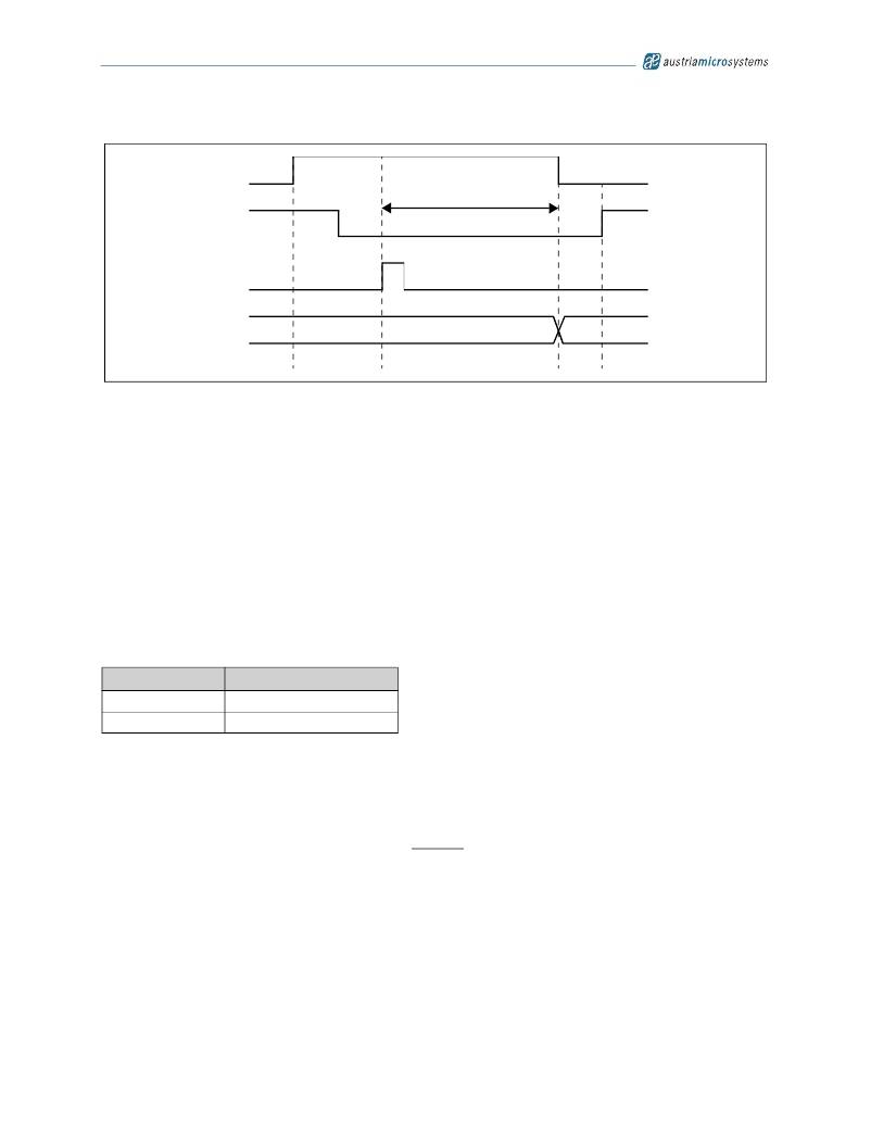
�Figure� 10.� Error� Detection� Timing� (GS=FFFF� HEX� ,� DC=3F� HEX� )�
�LD�
�>1μs�
�OEN�
�GSCLK�
�SID�
�Error�
�Detection�
�Start�
�LOD� n� ,� LSD� n�
�LOD� n+1� ,� LSD� n+1�
�Error�
�Detection�
�End�
�Note:� The� rising� edge� of� LD� latches� new� data� into� the� internal� registers� depending� on� the� logic� level� of� the� pin� MODE.� If� the� pin� MODE� is� tied�
�GND,� the� greyscale� registers� are� updated.� If� the� pin� MODE� is� tied� to� V� CC� ,� the� dot� correction� registers� are� updated.�
�Delay� Between� Outputs� (only� for� AS1112� and� AS1112B)�
�The� AS1112� uses� graduated� delay� circuits� between� OUT� n� outputs.� These� circuits� are� contained� in� the� constant-current� driver� block� of� the�
�AS1112� (see� Figure� 1� on� page� 1)� .� The� average-delay� time� is� 30ns� (typ).�
�The� maximum� delay� is� 450ns� (typ)� from� OUT0� to� OUT15.� The� delay� scheme� works� by� switching� on� and� switching� off� each� output� channel.� Thus�
�the� on/off� time� of� each� channel� is� the� same� regardless� of� the� delay.� These� delays� prevent� large� inrush� currents� and� switching� noise� that� can�
�reduce� bypass� capacitance� when� the� outputs� are� switched� on.�
�OUT� n� Enable�
�All� OUT� n� channels� can� be� collectively� switched� off� with� one� signal.� When� OEN� is� set� to� 1,� all� OUT� n� channels� are� disabled,� regardless� of� the�
�device� logic� operations.� The� greyscale� counter� is� also� reset� when� OEN� is� set� to� 1.�
�When� OEN� is� set� to� 0,� all� OUT� n� channels� are� in� normal� operation.�
�Table� 9.� Pin� OEN� Truth� Table�
�OEN�
�0�
�1�
�OUT0:OUT15�
�Normal� Operation�
�Disabled�
�Setting� Maximum� Channel� Current�
�The� maximum� output� current� per� channel� is� programmed� by� a� single� resistor,� R� IREF� ,� which� is� placed� between� pin� I� REF� and� GND.� The� voltage�
�on� pin� I� REF� is� set� by� an� internal� band� gap� V� IREF� (1.24V� typ).� The� maximum� channel� current� is� equivalent� to� the� current� flowing� through� R� IREF�
�multiplied� by� a� factor� of� 31.5.� The� maximum� output� current� is� calculated� as:�
�I� MAX� =�
�V� IREF�
�x� 31.5�
�(EQ� 1)�
�R� IREF�
�Where:�
�V� IREF� =� 1.24V;�
�R� IREF� =� User-selected� external� resistor.�
�Figure� 7� on� page� 7� shows� the� maximum� output� current� I� OUT� versus� R� IREF� ,� where� R� IREF� is� the� value� of� the� resistor� between� I� REF� terminal� to�
�GND,� and� I� OUT� is� the� constant� output� current� of� OUT0:OUT15.�
��Revision� 1.13�
�10� -� 19�
�相关PDF资料 |
PDF描述 |
|---|---|
| AS1115 DB-YELLOW | BOARD DEMO AS1115 YELLOW |
| AS1116 DB-YELLOW | BOARD DEMO AS1116 YELLOW |
| AS3691A EB | BOARD EVAL AS3691A |
| AS5030 DB | BOARD DEMO AS5030 |
| AS5048-DB-1.0 | BOARD DEMO AS5048 |
相关代理商/技术参数 |
参数描述 |
|---|---|
| AS1112-XXX-I-A1-D | 制造商:未知厂家 制造商全称:未知厂家 功能描述:Analog Filter |
| AS1112-XXX-I-A1-S | 制造商:未知厂家 制造商全称:未知厂家 功能描述:Analog Filter |
| AS1112-XXX-I-A2-D | 制造商:未知厂家 制造商全称:未知厂家 功能描述:Analog Filter |
| AS1112-XXX-I-A2-S | 制造商:未知厂家 制造商全称:未知厂家 功能描述:Analog Filter |
| AS1112-XXX-I-A3-D | 制造商:未知厂家 制造商全称:未知厂家 功能描述:Analog Filter |
发布紧急采购,3分钟左右您将得到回复。