- 您现在的位置:买卖IC网 > PDF目录14774 > AS1322B-BTTT (ams)IC REG BOOST SYNC ADJ TSOT23-6 PDF资料下载
参数资料
| 型号: | AS1322B-BTTT |
| 厂商: | ams |
| 文件页数: | 11/18页 |
| 文件大小: | 0K |
| 描述: | IC REG BOOST SYNC ADJ TSOT23-6 |
| 设计资源: | Design Support Tool |
| 标准包装: | 1 |
| 类型: | 升压(升压) |
| 输出类型: | 可调式 |
| 输出数: | 1 |
| 输出电压: | 2.5 V ~ 5 V |
| 输入电压: | 0.65 V ~ 5 V |
| PWM 型: | 电流模式 |
| 频率 - 开关: | 1.2MHz |
| 同步整流器: | 是 |
| 工作温度: | -40°C ~ 85°C |
| 安装类型: | 表面贴装 |
| 封装/外壳: | SOT-23-6 细型,TSOT-23-6 |
| 包装: | 标准包装 |
| 供应商设备封装: | TSOT-23-6 |
| 其它名称: | AS1322B-BTTTDKR |
�� �
�
�AS1322�
�Datasheet� -� A� p� p� l� i� c� a� t� i� o� n� I� n� f� o� r� m� a� t� i� o� n�
�9.1� Output� Voltage� Ripple�
�The� AS1322� is� designed� to� work� at� high� efficiency.� In� order� to� reduce� the� output� ripple� the� following� improvements� are� recommended:�
�Use� a� higher� output� capacitor,� up� to� 44μF� and� a� higher� input� capacitor� (22μF).�
�Use� smaller� values� for� the� resistor� divider.� R1� should� be� about� 300k� ?� .� To� avoid� a� high� leakage� current� from� pin� VOUT� through� the� resistor�
�divider� to� GND,� R1� should� not� be� less� than� 100k� ?� .�
�To� reduce� the� output� ripple� it’s� also� possible� to� speed� up� the� feedback� loop.� To� achieve� this,� place� a� 22pF� (C4� in� Figure� 20� )� capacitor� in�
�parallel� to� R1.� Via� C4� the� fast� transients� are� shorted� to� the� FB� pin� and� the� feedback� loop� is� even� faster.� A� 1M� ?� resistor� for� R1� slows� down�
�the� FB� loop.�
�Due� to� noise� and� to� their� non� linear� behavior,� the� use� of� potentiometers� is� not� recommended.�
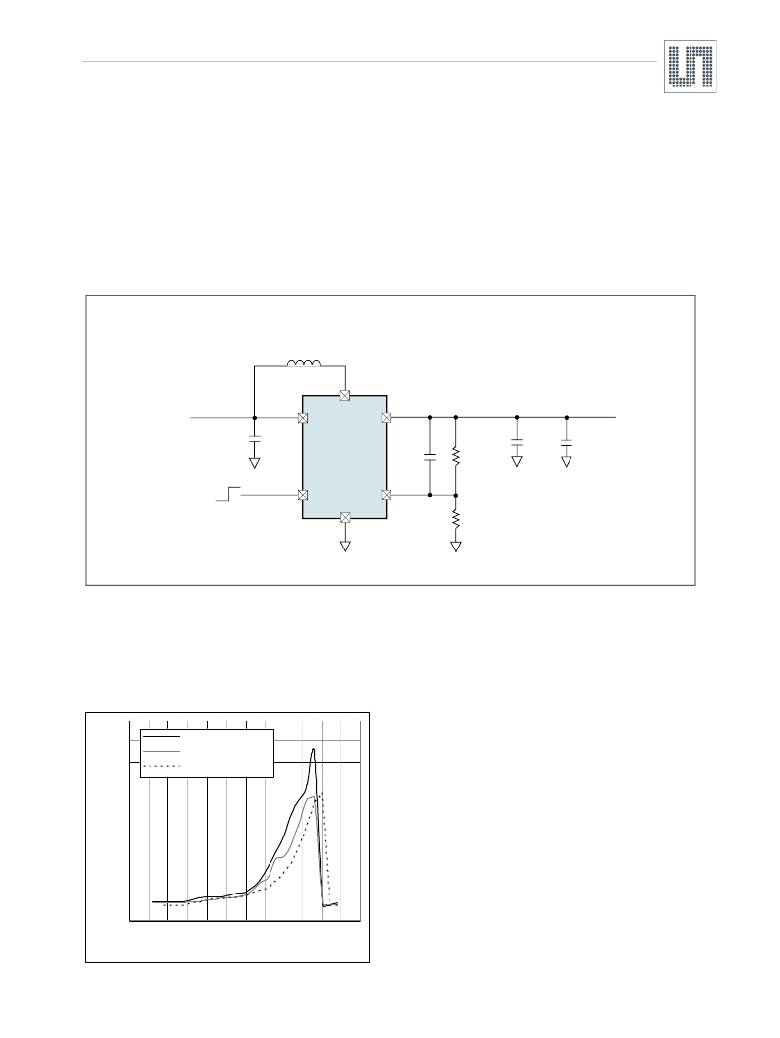
�Figure� 20.� AS1322� -� Typical� Application� for� lower� Output� Voltage� Ripple�
�L1�
�4.7μH�
�1�
�SW�
�2xAA� Battery�
�6�
�5�
�V� OUT� =� 2.8V�
�C� 1�
�22μF�
�VIN�
�AS1322�
�VOUT�
�C� 4�
�22pF�
�R� 1�
�250k� ?�
�C� 2�
�22μF�
�C� 3�
�22μF�
�On�
�4�
�3�
�Off�
�SHDNN�
�2�
�GND�
�FB�
�R� 2�
�196k� ?�
�Note:� For� correct� measurements� of� the� output� ripple� connect� the� oscilloscope� probe� as� close� as� possible� to� the� positive� plate� of� the� C� OUT�
�and� connect� the� GND� of� the� oscilloscope� probe� to� the� negative� plate� of� the� C� OUT� .� This� will� reduce� the� inductive� coupling� and� will�
�deliver� a� more� accurate� measurement� result.�
�The� output� ripple� is� getting� higher� as� V� IN� is� getting� closer� to� V� OUT� .� Figure� 21� shows� that� the� above� mentioned� improvements� reduce� the� output�
�voltage� ripple.� If� V� IN� is� higher� than� V� OUT� the� AS1322� stops� switching� and� V� IN� is� connected� to� V� OUT� via� the� inductor� and� the� internal� P-FET.�
�Figure� 21.� Output� Voltage� Ripple� vs.� Input� Voltage;� V� OUT� =� 2.8V,� I� OUT� =� 0.8mA�
�125�
�Cout� =� 44μF�
�Cout� =� 66μF�
�100�
�75�
�50�
�25�
�0�
�Cout� =� 44μF� +� C4� =� 22pF�
�0.5�
�1�
�1.5�
�2�
�2.5�
�3�
�3.5�
�Input� Voltage� (V)�
�www.ams.com/DC-DC_Step-Up/AS1322�
�Revision� 1.10�
�11� -� 18�
�相关PDF资料 |
PDF描述 |
|---|---|
| RCA40DTKN | CONN EDGECARD 80POS DIP .125 SLD |
| MAX6461XR22+T | IC VOLT DETECTOR LP SC70-3 |
| V110B15T150B3 | CONVERTER MOD DC/DC 15V 150W |
| V110B15T150B | CONVERTER MOD DC/DC 15V 150W |
| MAX6461XR29+T | IC VOLT DETECTOR LP SC70-3 |
相关代理商/技术参数 |
参数描述 |
|---|---|
| AS1322-EB | 制造商:ams 功能描述:AS1322 Evaluation Board |
| AS1-322-W3-302 | 制造商:TE Connectivity 功能描述: |
| AS1323 | 制造商:AMSCO 制造商全称:austriamicrosystems AG 功能描述:1.6uA Quiescent Current, Single Cell, DC-DC Step-up Converter |
| AS1323_04 | 制造商:AMSCO 制造商全称:austriamicrosystems AG 功能描述:1.6??A Quiescent Current, Single Cell, DC-DC Step-up Converter |
| AS1323_1 | 制造商:AMSCO 制造商全称:austriamicrosystems AG 功能描述:1.6uA Quiescent Current, Single Cell, DC-DC Step-up Converter |
发布紧急采购,3分钟左右您将得到回复。