- 您现在的位置:买卖IC网 > PDF目录14529 > AS1340A-BTDT-10-1K (ams)IC REG BOOST SYNC ADJ 1.4A 8TDFN PDF资料下载
参数资料
| 型号: | AS1340A-BTDT-10-1K |
| 厂商: | ams |
| 文件页数: | 10/17页 |
| 文件大小: | 0K |
| 描述: | IC REG BOOST SYNC ADJ 1.4A 8TDFN |
| 设计资源: | Design Support Tool |
| 标准包装: | 1 |
| 类型: | 升压(升压) |
| 输出类型: | 可调式 |
| 输出数: | 1 |
| 输出电压: | 2.7 V ~ 50 V |
| 输入电压: | 2.7 V ~ 50 V |
| 频率 - 开关: | 1MHz |
| 电流 - 输出: | 1.4A |
| 同步整流器: | 是 |
| 工作温度: | -40°C ~ 85°C |
| 安装类型: | 表面贴装 |
| 封装/外壳: | 8-WDFN 裸露焊盘 |
| 包装: | 标准包装 |
| 供应商设备封装: | 8-TDFN(3x3) |
| 其它名称: | AS1340A-BTDT-10-1KDKR |
�� �
�
�AS1340�
�Datasheet� -� A� p� p� l� i� c� a� t� i� o� n� I� n� f� o� r� m� a� t� i� o� n�
�9� Application� Information�
��The� AS1340� has� an� operating� voltage� range� from� 2.7� to� 5.5V.� If� the� inductor� is� supplied� from� the� same� source� the� battery� disconnect� switch� can�
�be� used� as� well� (see� Figure� 1� on� page� 1)� .� In� case� that� a� input� voltage� source� is� higher� than� 5.5V,� the� inductor� can� be� supplied� separately� up� to�
�50V� (see� Figure� 28)� ,� but� then� the� battery� disconnect� switch� cannot� be� used,� because� its� operating� voltage� range� is� limited� to� 5.5V.�
�9.2� Shutdown�
�A� logic� low� on� pin� EN� shuts� down� the� AS1340� and� a� logic� high� on� EN� powers� on� the� device.�
�In� shutdown� mode� the� supply� current� drops� to� below� 1μA� to� maximize� battery� life.� In� case� that� the� battery� disconnect� switch� is� used,� the� battery�
�is� disconnected� from� the� output� during� shutdown.�
�Note:� Pin� EN� should� not� be� left� floating.� If� the� shutdown� feature� is� not� used,� connect� EN� to� V� IN� .�
�9.3� Battery� Disconnect�
�The� AS1340� has� an� integrated� switch� that� can� be� used� to� disconnect� the� battery� during� shutdown.� The� operation� voltage� of� this� switch� is� limited�
�to� 5.5V.� When� EN� is� high,� the� switch� is� closed� and� supplies� the� inductor.� Due� to� the� R� ON� resistance� the� efficiency� is� slightly� lower� if� the� battery�
�disconnect� switch� is� used.�
�P� LOSS� =� I� IN� 2� x� R� ON�
�9.4� Setting� Output� Voltage�
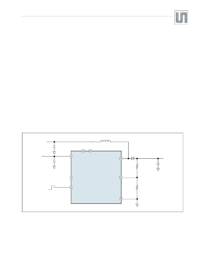
�Output� voltage� can� be� adjusted� by� connecting� a� voltage� divider� between� pins� LX� and� FB� (see� Figure� 28)� .�
�Figure� 28.� Typical� Application� (SWVIN� and� SWOUT� not� in� use)�
�Supply�
�(EQ� 1)�
�2.7V� to� V� OUT�
�C� IN�
�10μF�
�3�
�6�
�L� 1�
�4.7μH�
�V� IN� =� 2.7V�
�to� 5.5V�
�C� 1�
�0.1μF�
�2�
�VCC�
�SWVIN�
�SWOUT�
�5�
�LX�
�D1�
�R� 1�
�2.2M� ?�
�C� OUT�
�1μF�
�V� OUT� =� 18V�
�4�
�POK�
�AS1340�
�8�
�FB�
�On�
�Off�
�1�
�EN�
�R� 2�
�165k� ?�
�7,9�
�GND�
�The� output� voltage� can� be� adjusted� by� selecting� different� values� for� R� 1� and� R� 2� .� For� R� 2� ,� select� a� value� between� 10k� and� 200k� ?� .�
�Calculate� R� 1� by:�
�R� 1� =� R� 2� ?� ?� -------------� –� 1� ?�
�?� V� FB�
�V� OUT�
�?�
�(EQ� 2)�
�Where:�
�V� OUT� =� V� IN� to� 50V,� V� FB� =� 1.25V�
�The� input� bias� current� of� FB� has� a� maximum� value� of� 100nA� which� allows� for� large-value� resistors.� For� less� than� 1%� error,� the� current� through� R� 2�
�should� be� 100� times� the� feedback� input� bias� current� (I� FB� ).�
�www.ams.com/DC-DC_Step-Up/AS1340�
�Revision� 1.20�
�10� -� 17�
�相关PDF资料 |
PDF描述 |
|---|---|
| GBB60DHNN-S621 | CONN EDGECARD 120POS .050 SOLDER |
| GBB60DHND-S621 | CONN EDGECARD 120POS .050 SOLDER |
| GBB60DHHN-S621 | CONN EDGECARD 120POS .050 SOLDER |
| GBB60DHHD-S621 | CONN EDGECARD 120POS .050 SOLDER |
| GBB60DHHN-S578 | CONN EDGECARD 120POS .050 SLD |
相关代理商/技术参数 |
参数描述 |
|---|---|
| AS1340ABTDT10-1K | 制造商:ams 功能描述:TDFN 8 |
| AS1340A-BTDT-10-6K | 功能描述:IC REG BOOST SYNC ADJ 1.4A 8TDFN RoHS:是 类别:集成电路 (IC) >> PMIC - 稳压器 - DC DC 开关稳压器 系列:- 标准包装:50 系列:- 类型:升压(升压) 输出类型:可调式 输出数:1 输出电压:5 V ~ 25 V 输入电压:2.3 V ~ 5.5 V PWM 型:电流模式 频率 - 开关:600kHz,1.2MHz 电流 - 输出:1A 同步整流器:无 工作温度:-40°C ~ 85°C 安装类型:表面贴装 封装/外壳:8-TSSOP,8-MSOP(0.118",3.00mm 宽) 包装:管件 供应商设备封装:8-MSOP |
| AS1340A-TD-10_EK_S | 功能描述:AS1340 - DC/DC, Step Up 1, Non-Isolated Outputs Evaluation Board 制造商:ams 系列:- 零件状态:在售 主要用途:DC/DC,步升 输出和类型:1,非隔离 功率 - 输出:- 电压 - 输出:2.7 V ~ 50 V 电流 - 输出:100mA 电压 - 输入:2.7 V ~ 5.5 V 稳压器拓扑:升压 频率 - 开关:1MHz 板类型:完全填充 所含物品:板 使用的 IC/零件:AS1340 标准包装:1 |
| AS1340A-TD-10_EK_ST | 功能描述:AS1340 - DC/DC, Step Up 1, Non-Isolated Outputs Evaluation Board 制造商:ams 系列:- 零件状态:有效 主要用途:DC/DC,步升 输出和类型:1,非隔离 功率 - 输出:- 电压 - 输出:2.7 V ~ 50 V 电流 - 输出:100mA 电压 - 输入:2.7 V ~ 5.5 V 稳压器拓扑:升压 频率 - 开关:1MHz 板类型:完全填充 所含物品:板 使用的 IC/零件:AS1340 标准包装:1 |
| AS1341 | 制造商:AMSCO 制造商全称:austriamicrosystems AG 功能描述:20V, 600mA, 100% Duty Cycle, Step-Down Converter |
发布紧急采购,3分钟左右您将得到回复。