- 您现在的位置:买卖IC网 > PDF目录255362 > AS2320-9RD3TB1 2-OUTPUT 100 W DC-DC REG PWR SUPPLY MODULE PDF资料下载
参数资料
| 型号: | AS2320-9RD3TB1 |
| 元件分类: | 电源模块 |
| 英文描述: | 2-OUTPUT 100 W DC-DC REG PWR SUPPLY MODULE |
| 封装: | METAL, CASE S02, MODULE |
| 文件页数: | 22/31页 |
| 文件大小: | 633K |
| 代理商: | AS2320-9RD3TB1 |
第1页第2页第3页第4页第5页第6页第7页第8页第9页第10页第11页第12页第13页第14页第15页第16页第17页第18页第19页第20页第21页当前第22页第23页第24页第25页第26页第27页第28页第29页第30页第31页
Cassette Style
100 Watt DC-DC Converters
S Series
Edition 1/01.2000
29/31
V ACFAIL Signal (VME)
Available for units with Uo1 = 5.1V
This option defines an undervoltage monitoring circuit for
the input or input and main output voltage (
Uo1 nom =5.1 V
only) equivalent to option D and generates an ACFAIL sig-
nal (V signal) which conforms to the VME standard.
The low state level of the ACFAIL signal is specified at a
sink current of
IV ≤ 48 mA to UV ≤ 0.6 V (open-collector out-
put of a NPN transistor). The pull-up resistor feeding the
open-collector output should be placed on the VME back
plane. After the ACFAIL signal has gone low, the VME
standard requires a hold-up time
th of at least 4 ms before
the 5.1 V output drops to 4.875 V when the output is fully
loaded. This hold-up time
th is provided by the internal input
capacitance. Consequently the working input voltage and
the threshold level
Uti should be adequately above the
minimum input voltage
Ui min of the converter so that
enough energy is remaining in the input capacitance. If the
input voltage is below the required level, an external hold-
up capacitor (
Ci ext) should be added.
Formula for threshold level for desired value of
th:
2
Po (th + 0.3 ms) 100
Uti =
––––––––––––––––––––– +
Ui min2
Ci min h
V output (V0, V2, V3):
Connector pin V is internally connected to the open collec-
tor of a NPN transistor. The emitter is connected to the
negative potential of output 1.
UV
≤ 0.6 V (logic low) corre-
sponds to a monitored voltage level (
Ui and/or Uo1) <Ut.
The current
I V through the open collector should not exceed
50 mA. The NPN output is not protected against external
overvoltages.
UV should not exceed 60 V.
Ui, Uo1 status
V output,
UV
Ui or Uo1 < Ut
low, L,
UV ≤ 0.6 V at IV = 50 mA
Ui and Uo1 > Ut + Uh
high, H,
IV ≤ 25 A at UV = 5.1 V
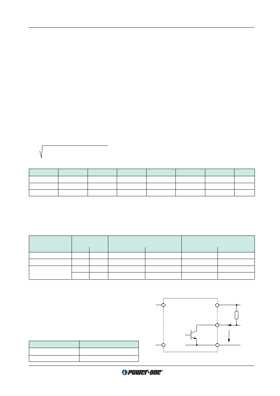
Fig. 34
Output configuration of options V0, V2 and V3
Vo1+
Vo1–
V
UV
IV
Rp
Input
11009
Table 20: Undervoltage monitor functions
V output
Monitoring
Minimum adjustment range
Typical hysteresis
Uh [% of Ut]
(VME compatible)
of threshold level
for Ut min…Ut max
Ui
Uo1
Uti
Uto
Uhi
Uho
V2
yes
no
Ui min...Ui max 1
–
3.4...0.4
–
V3
yes
Ui min...Ui max 1
0.95...0.985
Uo1 2
3.4...0.4
"0"
V0
yes
no
Ui min...Ui max 3 4
–
3.4...0.4
–
yes
Ui min...Ui max 3 4
0.95...0.985
Uo1 2
3.4...0.4
"0"
1 Threshold level adjustable by potentiometer. 2 Fixed value between 95% and 98% of Uo1 (tracking). 3 Adjusted at Io nom.
4 Fixed value, resistor-adjusted (
±2% at 25°C) acc. to customer's specifications; individual type number is determined by Power-One.
voltage(s) exceed(s)
Ut + Uh. The threshold level Uti is ei-
ther adjustable by potentiometer, accessible through a hole
in the front cover, or adjusted during manufacture to a de-
termined customer specified value.
Versions V0, V2 and V3 are available as shown below.
Option V operates independently of the built-in input under-
voltage lock-out circuit. A logic "low" signal is generated at
pin 20 as soon as one of the monitored voltages drops be-
low the preselected threshold level
Ut. The return for this
signal is Vo1–. The V output recovers when the monitored
Table 19: Available internal input capacitance and factory potentiometer setting of Ut i with resulting hold-up time
Types
ASBS
FS
CSDS
ES
Unit
Ci min
0.83
0.3
1.2
0.66
0.26
0.21
mF
Uti
9.5
19.5
393961
97
V DC
th
0.1
5.3
1.9
1.8
4.3
ms
Formula for the external input capacitor:
2
Po (th + 0.3 ms) 100
Ci ext = –––––––––––––––––––––– – Ci min
h (Uti 2 – Ui min2)
where as:
Ci min = internal input capacitance [mF]
Ci ext = external input capacitance [mF]
Po
= output power [W]
h
= efficiency [%]
th
= hold-up time [ms]
Ui min = minimum input voltage [V] 1
Uti
= threshold level [V]
1 Min. input voltage according to Electrical Input Data. For output
voltages
Uo > Uo nom, the minimum input voltage increases pro-
portionally to
Uo/Uo nom.
Remarks:
Option V2 and V3 can be adjustment by potentiometer to a
threshold level between
Ui min and Ui max. A decoupling di-
ode should be connected in series with the input of AS...FS
converters to avoid the input capacitance discharging
through other loads connected to the same source voltage.
相关PDF资料 |
PDF描述 |
|---|---|
| AS2320-9RD5B2 | 2-OUTPUT 100 W DC-DC REG PWR SUPPLY MODULE |
| AS2540-9PD8TB1 | 2-OUTPUT 100 W DC-DC REG PWR SUPPLY MODULE |
| AS2660-7PD8TB1 | 2-OUTPUT 100 W DC-DC REG PWR SUPPLY MODULE |
| AS2660-7RD3B2 | 2-OUTPUT 100 W DC-DC REG PWR SUPPLY MODULE |
| AM1501-7PV2F | 1-OUTPUT 50 W DC-DC REG PWR SUPPLY MODULE |
相关代理商/技术参数 |
参数描述 |
|---|---|
| AS23240FLF | 制造商:TT Electronics / IRC 功能描述:AS23240FLF |
| AS23240HLF | 制造商:TT Electronics / IRC 功能描述:AS23240HLF |
| AS23240JLF | 制造商:TT Electronics / IRC 功能描述:AS23240JLF |
| AS23241FLF | 制造商:TT Electronics / IRC 功能描述:AS23241FLF |
| AS23241HLF | 制造商:TT Electronics / IRC 功能描述:AS23241HLF |
发布紧急采购,3分钟左右您将得到回复。