- 您现在的位置:买卖IC网 > PDF目录11670 > AS8510-ASST-500 (ams)IC BATTERY MANAGEMENT 20-SSOP PDF资料下载
参数资料
| 型号: | AS8510-ASST-500 |
| 厂商: | ams |
| 文件页数: | 10/47页 |
| 文件大小: | 0K |
| 描述: | IC BATTERY MANAGEMENT 20-SSOP |
| 产品培训模块: | AS8510 Data Acquisition IC |
| 标准包装: | 1 |
| 类型: | 电池管理 |
| 输入类型: | 模拟,数字 |
| 输出类型: | 模拟,数字 |
| 接口: | SPI 串行 |
| 电流 - 电源: | 5.5mA |
| 安装类型: | 表面贴装 |
| 封装/外壳: | 20-SSOP(0.209",5.30mm 宽) |
| 供应商设备封装: | 20-SSOP |
| 包装: | 标准包装 |
| 其它名称: | AS8510-ASST-500DKR |
第1页第2页第3页第4页第5页第6页第7页第8页第9页当前第10页第11页第12页第13页第14页第15页第16页第17页第18页第19页第20页第21页第22页第23页第24页第25页第26页第27页第28页第29页第30页第31页第32页第33页第34页第35页第36页第37页第38页第39页第40页第41页第42页第43页第44页第45页第46页第47页
Revision 3.5
17 - 46
AS8510
Datasheet - Detailed Descr i p ti on
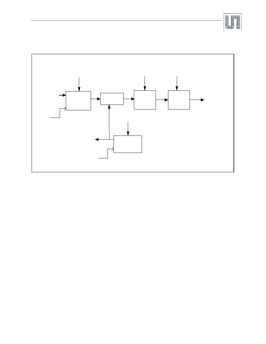
7.3 Digital Implementation of Measurement Path
Figure 3. Block Diagram of Digital Implementation
Figure 3 shows the digital implementation of the decimator and filter to process the 1-bit output of the Modulator. This block receives a 1-bit pulse
density modulated output (MOD_IN) from the second order sigma delta modulator along with the oversampling frequency clock (MOD_CLK).
The MOD_CLK directly goes to a clock division block, which generates chopper clock (CHOP_CLK). The CHOP_CLK can be one of 2kHz or
4kHz selected by Register CLK_REG in Table 33. The MOD_CLK can be either 1MHz or 2MHz. The Decimation is a two phase process. In the
first phase, the R1 down sampling rate can be obtained by selecting either 64 or 128 in Registers DECREG_R1_I, DECREG_R1_V in Table 33.
The 16-bit CIC1 output is dechopped with respect to CHOP_CLK. The output of Dechopper is passed through the CIC2 filter with a decimation
ratio of 1to 32768 in steps of power of 2. This output is then processed through a FIR or Moving Average (MA) filter. FIR Filter is provided to offer
matched low pass filter response typically required in lead acid battery sensor systems. MA filter is used to provide averaged output and the
number of samples for averaging can be any integer value from 1 to 15.
7.4 Modes of Operation
The device operates in four different modes, namely,
Normal Mode 1 (NOM1),
Normal Mode 2 (NOM2),
Standby Mode 1 (SBY1), and,
Standby Mode 2 (SBY2).
The Normal Modes are full-power modes with the exception that in Normal Mode 2, sampling is normally at a programmed lower frequency and
is increased to a higher rate only when a measured input signal level crosses the programmed threshold in the current measurement channel.
The Standby Modes are lower power modes. Sampling is normally at a very low frequency interval. In Standby Mode 2, data sampling can be
carried out only when the internal comparator detects the input current to be greater than the programmed threshold and it generates interrupt on
the INT pin.
The device enters into the “Stop” state on Power On. This is a state where in the data path is inactive and can be entered into from any of the
four Modes. The State transition Diagram involving the state of Stop and the four Modes is illustrated in the Figure 4.
CIC1
64/ 128
CLKDIVISION
BLOCK
Dechopper
FIR/MA
MOD_IN
MOD_CLK
DATAOUT
R1
R1=First decimationratio(64or 128)
R2=Seconddecimationratio(1to32768)
MOD_CLK
R1
CIC2
R2
FIR_MA_SEL
CHP_CLK
fmod / R1
fchop * 2
fchop * 2/ R2
fchop
fmod
fchop * 2/ R2
相关PDF资料 |
PDF描述 |
|---|---|
| VI-BTF-IX-F3 | CONVERTER MOD DC/DC 72V 75W |
| VE-J3N-IZ-B1 | CONVERTER MOD DC/DC 18.5V 25W |
| NCV1124DR2G | IC SENSOR DUAL VAR-RELUCT 8-SOIC |
| MS27508E24B1PB | CONN RCPT 128POS BOX MNT W/PINS |
| D38999/26WJ4PN | CONN PLUG 56POS STRAIGHT W/PINS |
相关代理商/技术参数 |
参数描述 |
|---|---|
| AS8510-COPPER-SHUNT | 功能描述:DEMO BOARD FOR AS8510 制造商:ams 系列:- 零件状态:在售 主要用途:接口,数据捕捉 嵌入式:- 使用的 IC/零件:AS8510 主要属性:- 辅助属性:图形用户界面 所含物品:板 标准包装:1 |
| AS8510-DB | 制造商:ams 功能描述:AS8510 Demo Board |
| AS8515-ZMFM | 制造商:ams 功能描述:IC BATTERY MANAGEMENT 制造商:ams 功能描述:Data Acquisition System w/ Power Management and LIN Transceiver - MLF-32 制造商:ams 功能描述:T&R / MLF 32 (5x5) |
| AS8515-ZMFP | 制造商:ams 功能描述:IC INTERFACE TRANSCEIVER 制造商:ams 功能描述:T&R / MLF 32 (5x5) |
| AS8520 | 制造商:AMSCO 制造商全称:austriamicrosystems AG 功能描述:LIN Transceiver with Voltage Regulator, Attenuator, Relay Drivers, MCU Interface for Automotive Applications |
发布紧急采购,3分钟左右您将得到回复。