- 您现在的位置:买卖IC网 > PDF目录11670 > AS8510-ASST-500 (ams)IC BATTERY MANAGEMENT 20-SSOP PDF资料下载
参数资料
| 型号: | AS8510-ASST-500 |
| 厂商: | ams |
| 文件页数: | 13/47页 |
| 文件大小: | 0K |
| 描述: | IC BATTERY MANAGEMENT 20-SSOP |
| 产品培训模块: | AS8510 Data Acquisition IC |
| 标准包装: | 1 |
| 类型: | 电池管理 |
| 输入类型: | 模拟,数字 |
| 输出类型: | 模拟,数字 |
| 接口: | SPI 串行 |
| 电流 - 电源: | 5.5mA |
| 安装类型: | 表面贴装 |
| 封装/外壳: | 20-SSOP(0.209",5.30mm 宽) |
| 供应商设备封装: | 20-SSOP |
| 包装: | 标准包装 |
| 其它名称: | AS8510-ASST-500DKR |
第1页第2页第3页第4页第5页第6页第7页第8页第9页第10页第11页第12页当前第13页第14页第15页第16页第17页第18页第19页第20页第21页第22页第23页第24页第25页第26页第27页第28页第29页第30页第31页第32页第33页第34页第35页第36页第37页第38页第39页第40页第41页第42页第43页第44页第45页第46页第47页
Revision 3.5
19 - 46
AS8510
Datasheet - Detailed Descr i p ti on
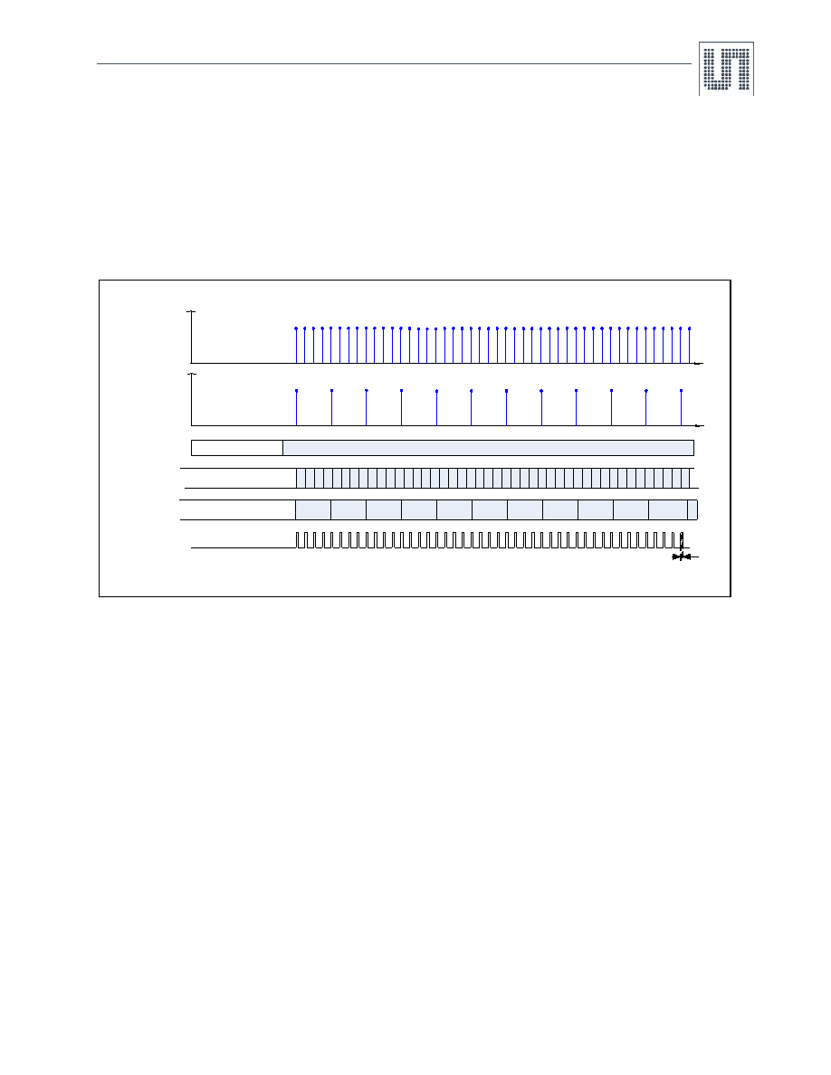
7.4.1 Normal Mode 1 (NOM1)
On Power-on-reset of the device, AS8510 goes into STOP State.
Transition to Normal mode1 (NOM1) occurs when the “START BIT” D0 of Mode Control Register MOD_CTL_REG in Table 33 is set to “1”
through the serial port SPI. Data Rate of voltage and current channels can be independently programmed and both the channels generate
interrupts for every output available from ADC. The interrupt signal is generated on the INT pin. The width of the interrupt pulse is eight cycles of
lp_clk. The data is stable up to the next interrupt. If the data rate is different for the two channels, the interrupt rate would follow the higher rate
among the two channels. Data update can be known by reading the status register. The functionality is explained in the waveform shown in
Figure 5. When the device is configured to NORMAL Mode1 from any mode the configuration should be through the STOP state only.
Figure 5. Normal Mode 1
7.4.2 Normal Mode 2 (NOM2)
NOM2 differs from NOM1 in such a way that it allows for a relaxed data rate at a period of TMC by programming the corresponding register as
long as the amplitude of current is less than a programmed threshold ITHC. However, when, the measured input signal exceeds the programmed
threshold, the data rate is changed to the rate of NOM1 mode.
Transition to NOM2 occurs when the “START BIT” D0 of Mode Control register MOD_CTL_REG in Table 33 is set to 1 and mode control bits to
01 through SPI. In this mode the data rate should be programmed with the time of TMC. An interrupt signal is generated on INT at the rate of TMC
secs with a pulse width of eight cycles of lp_clk. The data is stable up to the next interrupt. The data sample is compared against the programmed
threshold and when it is exceeded, the data sampling rate is changed to provide data at the data rate of NOM1 mode. However, as soon as the
data sample amplitude falls below the programmed threshold, the sampling rate is restored to provide data at the rate of TMC. The functionality is
illustrated in the waveform Figure 6.
Sampling with f1
INT at f1 rate from
current channel
Current Channel
DATA Register
t
I
START
STOP
t
V,T
Sampling with f2
Voltage Channel
DATA Register
Interrupt fromthe current channel is at f1 rate which is integer multiple of f2 rate fromvoltage channel
IDATA
V,TDATA
TINT
相关PDF资料 |
PDF描述 |
|---|---|
| VI-BTF-IX-F3 | CONVERTER MOD DC/DC 72V 75W |
| VE-J3N-IZ-B1 | CONVERTER MOD DC/DC 18.5V 25W |
| NCV1124DR2G | IC SENSOR DUAL VAR-RELUCT 8-SOIC |
| MS27508E24B1PB | CONN RCPT 128POS BOX MNT W/PINS |
| D38999/26WJ4PN | CONN PLUG 56POS STRAIGHT W/PINS |
相关代理商/技术参数 |
参数描述 |
|---|---|
| AS8510-COPPER-SHUNT | 功能描述:DEMO BOARD FOR AS8510 制造商:ams 系列:- 零件状态:在售 主要用途:接口,数据捕捉 嵌入式:- 使用的 IC/零件:AS8510 主要属性:- 辅助属性:图形用户界面 所含物品:板 标准包装:1 |
| AS8510-DB | 制造商:ams 功能描述:AS8510 Demo Board |
| AS8515-ZMFM | 制造商:ams 功能描述:IC BATTERY MANAGEMENT 制造商:ams 功能描述:Data Acquisition System w/ Power Management and LIN Transceiver - MLF-32 制造商:ams 功能描述:T&R / MLF 32 (5x5) |
| AS8515-ZMFP | 制造商:ams 功能描述:IC INTERFACE TRANSCEIVER 制造商:ams 功能描述:T&R / MLF 32 (5x5) |
| AS8520 | 制造商:AMSCO 制造商全称:austriamicrosystems AG 功能描述:LIN Transceiver with Voltage Regulator, Attenuator, Relay Drivers, MCU Interface for Automotive Applications |
发布紧急采购,3分钟左右您将得到回复。