- 您现在的位置:买卖IC网 > PDF目录166232 > AS8F128K32Q-150/883C (AUSTIN SEMICONDUCTOR INC) 128K x 32 FLASH FLASH MEMORY ARRAY PDF资料下载
参数资料
| 型号: | AS8F128K32Q-150/883C |
| 厂商: | AUSTIN SEMICONDUCTOR INC |
| 元件分类: | PROM |
| 英文描述: | 128K x 32 FLASH FLASH MEMORY ARRAY |
| 中文描述: | 128K X 32 FLASH 5V PROM MODULE, 150 ns, CQFP68 |
| 封装: | CERAMIC, QFP-68 |
| 文件页数: | 22/22页 |
| 文件大小: | 1260K |
| 代理商: | AS8F128K32Q-150/883C |
FLASH
AS8F128K32
AS8F128K32
Rev. 2.7 09/07
Austin Semiconductor, Inc. reserves the right to change products or specifications without notice.
9
Austin Semiconductor, Inc.
WRITE OPERATION STATUS
The device provides several bits to determine the status of
a write operation: I/O3, I/O5, I/O6, and I/O7. Table 5 and the
following subsections describe the functions of these bits.
I/O7 and I/O6 each offer a method for determining whether a
program or erase operation is complete or in progress. These
three bits are discussed first.
I/O7: Data\ Polling
The Data\ Polling bit, I/O7*, indicates to the host system
whether an Embedded Algorithm is in progress or completed.
Data\ Polling is valid after the rising edge of the final WEx\
pulse in the program or erase command sequence.
During the Embedded Program algorithm, the device
outputs on I/O7* the complement of the datum programmed to
I/O7*. When the Embedded Program algorithm is complete, the
device outputs the datum programmed to I/O7*. The system
must provide the program address to read valid status
information on I/O7*. If a program address falls within a
protected sector, Data\ Polling on I/O7* is active for
approximately 2 ms, then the device returns to reading array
data.
During the Embedded Erase algorithm, Data\ Polling
produces a “0” on I/O7*. When the Embedded Erase algorithm
is complete, Data\ Polling produces a “1” on I/O7*. This is
analogous to the complement/true datum output described for
the Embedded Program algorithm: the erase function changes
all the bits in a sector to “1”; prior to this, the device outputs
the “complement,” or “0.” The system must provide an address
within any of the sectors selected for erasure to read valid
status information on I/O7*.
After an erase command sequence is written, if all sectors
selected for erasing are protected, Data\ Polling on I/O7* is
active for approximately 100 ms, then the device returns to
reading array data. If not all selected sectors are protected, the
Embedded Erase algorithm erases the unprotected sectors, and
ignores the selected sectors that are protected.
When the system detects I/O7* has changed from the
complement to true data, it can read valid data at I/O7– I/O0 on
the following read cycles. This is because I/O7* may change
asynchronously with I/O0–I/O6 while Output Enable (OE\) is
asserted low. The Data\ Polling Timings (During Embedded
Algorithms) figure in the “AC Characteristics” section
illustrates this. Table 5 shows the outputs for Data\ Polling on
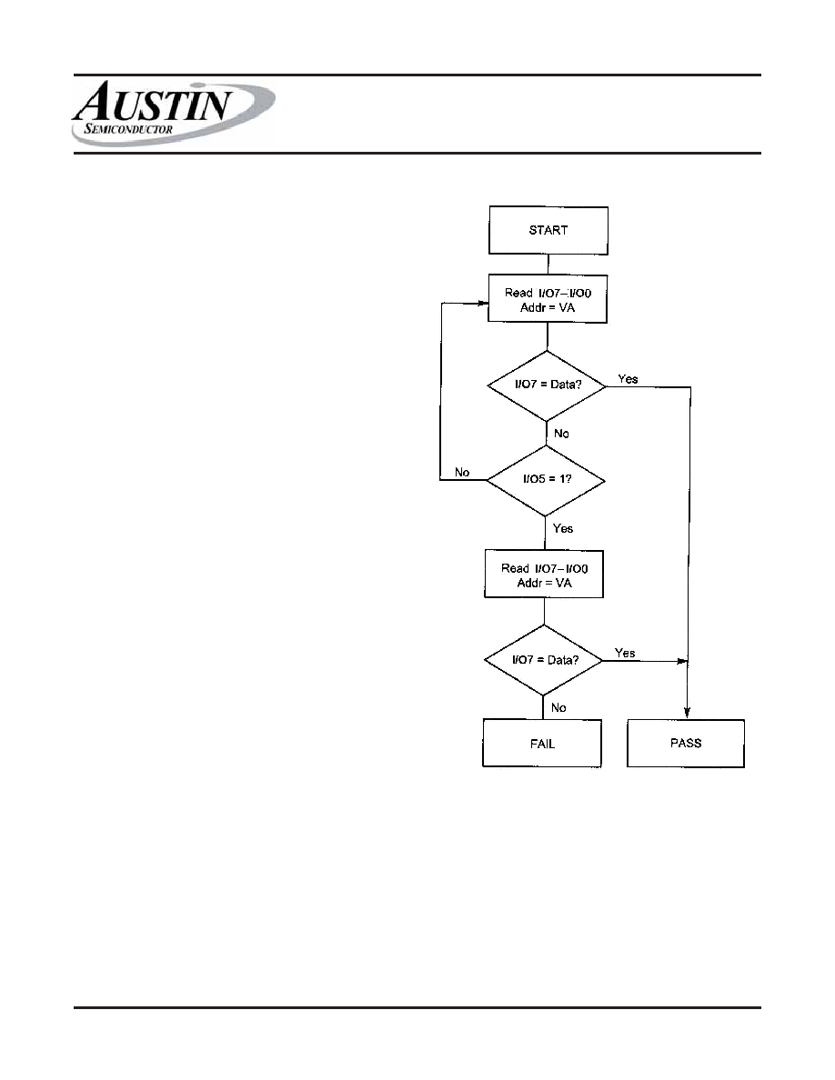
I/O7*. Figure 3 shows the Data\ Polling algorithm.
FIGURE 3: Data\ Polling Algorithm
NOTES:
1. VA = Valid address for programming. During a sector erase operation,
a valid address is an address within any sector selected for erasure. During
chip erase, a valid address is any non-protected sector address.
2. I/O7 should be rechecked even if I/O5 = “1” because I/O7 may change
simultaneously with I/O5.
*NOTE: applies to every 8th byte.
*
相关PDF资料 |
PDF描述 |
|---|---|
| AS8F128K32Q-150/IT | 128K x 32 FLASH FLASH MEMORY ARRAY |
| AS8F128K32Q-150/Q | 128K x 32 FLASH FLASH MEMORY ARRAY |
| AS8F128K32Q-150/XT | 128K x 32 FLASH FLASH MEMORY ARRAY |
| AS8F128K32Q1-60/883C | 128K x 32 FLASH FLASH MEMORY ARRAY |
| AS8F128K32Q1-60/IT | 128K x 32 FLASH FLASH MEMORY ARRAY |
相关代理商/技术参数 |
参数描述 |
|---|---|
| AS8F128K32Q1-60/883C | 制造商:AUSTIN 制造商全称:Austin Semiconductor 功能描述:128K x 32 FLASH FLASH MEMORY ARRAY |
| AS8F128K32Q1-60/IT | 制造商:Micross Components 功能描述:FLASH-MCM,4 MB - Trays |
| AS8F128K32Q1-60/Q | 制造商:Micross Components 功能描述:FLASH-MCM,4 MB - Trays |
| AS8F128K32Q1-60/XT | 制造商:AUSTIN 制造商全称:Austin Semiconductor 功能描述:128K x 32 FLASH FLASH MEMORY ARRAY |
| AS8F128K32Q1-70/883C | 制造商:AUSTIN 制造商全称:Austin Semiconductor 功能描述:128K x 32 FLASH FLASH MEMORY ARRAY |
发布紧急采购,3分钟左右您将得到回复。