- 您现在的位置:买卖IC网 > PDF目录166232 > AS8F128K32Q-150/Q (AUSTIN SEMICONDUCTOR INC) 128K x 32 FLASH FLASH MEMORY ARRAY PDF资料下载
参数资料
| 型号: | AS8F128K32Q-150/Q |
| 厂商: | AUSTIN SEMICONDUCTOR INC |
| 元件分类: | PROM |
| 英文描述: | 128K x 32 FLASH FLASH MEMORY ARRAY |
| 中文描述: | 128K X 32 FLASH 5V PROM MODULE, 150 ns, CQFP68 |
| 封装: | CERAMIC, QFP-68 |
| 文件页数: | 3/22页 |
| 文件大小: | 1260K |
| 代理商: | AS8F128K32Q-150/Q |
FLASH
AS8F128K32
AS8F128K32
Rev. 2.7 09/07
Austin Semiconductor, Inc. reserves the right to change products or specifications without notice.
11
Austin Semiconductor, Inc.
I/O5: Exceeded Timing Limits
I/O5* indicates whether the program or erase time has
exceeded a specified internal pulse count limit. Under these
conditions I/O5* produces a “1.” This is a failure condition
that indicates the program or erase cycle was not successfully
completed.
The I/O5* failure condition may appear if the system tries
to program a “1” to a location that is previously programmed to
“0.” Only an erase operation can change a “0” back to a “1.”
Under this condition, the device halts the operation, and when
the operation has exceeded the timing limits, I/O5* produces a
“1.” Under both these conditions, the system must issue the
reset command to return the device to reading array data.
I/O3: Sector Erase Timer
After writing a sector erase command sequence, the
system may read I/O3* to determine whether or not an erase
operation has begun. (The sector erase timer does not apply to
the chip erase command.) If additional sectors are selected for
erasure, the entire timeout also applies after each additional
sector erase command. When the time-out is complete, I/O3*
switches from “0” to “1.” The system may ignore I/O3* if the
system can guarantee that the time between additional sector
erase commands will always be less than 50 ms. See also the
“Sector Erase Command Sequence” section.
After the sector erase command sequence is written, the
system should read the status on I/O7* (Data\ Polling) or I/O6
(Toggle Bit I) to ensure the device has accepted the command
sequence, and then read I/O3. If I/O3 is “1”, the internally
controlled erase cycle has begun; all further commands are
ignored until the erase operation is complete. If I/O3 is “0”, the
device will accept additional sector erase commands. To
ensure the command has been accepted, the system software
should check the status of I/O3 prior to and following each
subsequent sector erase command. If I/O3 is high on the
second status check, the last command might not have been
accepted. Table 5 shows the outputs for I/O3.
TABLE 5: Write Operation Status
OPERATION
I/O7
1,*
I/O6*
I/O5
2,*
I/O3*
Embedded Program Algorithm
I/O7\
Toggle
0
N/A
Embedded Erase Algorithm
0
Toggle
0
1
NOTES: *applies to every 8th byte
1. I/O7 requires a valid address when reading status information. Refer to the appropriate subsection for further details.
2. I/O5 switches to ‘1’ when an Embedded Program or Embedded Erase operation has exceeded the maximum timing limits. See “I/O5: Exceeded
Timing Limits” for more information.
*Stresses greater than those listed under "Absolute Maximum
Ratings" may cause permanent damage to the device. This is
a stress rating only and functional operation of the device at
these or any other conditions above those indicated in the
operation section of this specification is not implied. Exposure
to absolute maximum rating conditions for extended periods
may affect reliability.
ABSOLUTE MAXIMUM RATINGS*
Voltage with respect to Ground, V
CC
1.........................-2.0Vto +7.0V
Voltage with respect to Ground,A9
2..........................-2.0Vto +14V
Voltage with respect to Ground, All other pins
1......-2.0V to +7.0V
Short-circuit output current.....................................................200mA
Ambient Temperature with powerApplied...............-55°C to 125°C
Storage temperature range..........................................-65°C to 150°C
NOTES:
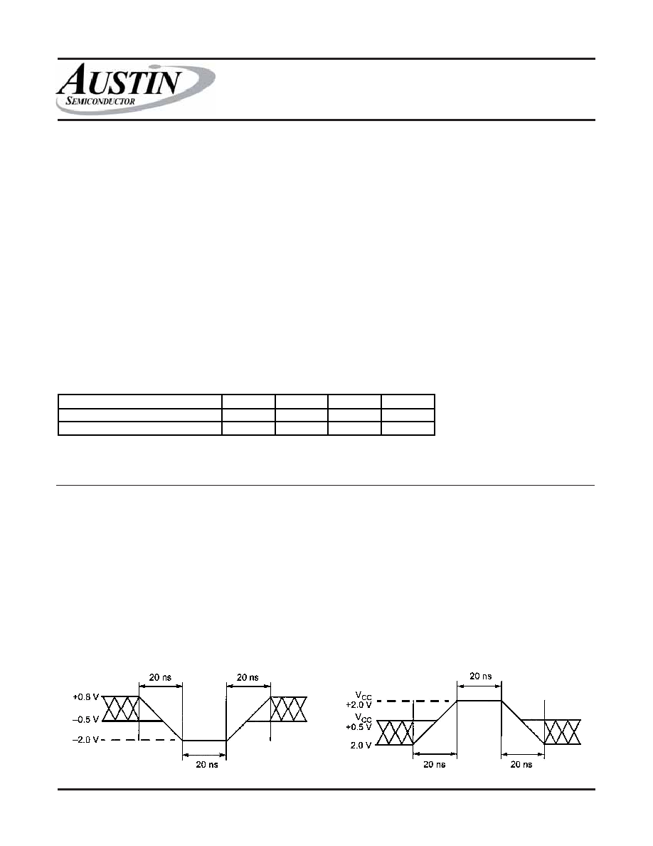
1. Minimum DC voltage on input or I/O pin is –0.5 V. During voltage transitions, inputs may overshoot V
SS to –2.0 V for periods of up to 20 ns. See
Figure 5. Maximum DC on input and I/O pins is V
CC + 0.5 V. During voltage transitions, input and I/O pins may overshoot to VCC + 2.0 V for periods
up to 20 ns. See Figure 6.
2. Minimum DC input voltage on A9 pin is –0.5V. During voltage transitions, A9 pins may overshoot V
SS to –2.0 V for periods of up to 20 ns. See
Figure 5. Maximum DC input voltage on A9 is +12.5 V which may overshoot to 14V for periods up to 20 ns.
3. No more than one output shorted at a time. Duration of the short circuit should not be greater than one second.
FIGURE 5: Maximum Negative Overshoot
FIGURE 6: Maximum Positive Overshoot
相关PDF资料 |
PDF描述 |
|---|---|
| AS8F128K32Q-150/XT | 128K x 32 FLASH FLASH MEMORY ARRAY |
| AS8F128K32Q1-60/883C | 128K x 32 FLASH FLASH MEMORY ARRAY |
| AS8F128K32Q1-60/IT | 128K x 32 FLASH FLASH MEMORY ARRAY |
| AS8F128K32Q1-60/Q | 128K x 32 FLASH FLASH MEMORY ARRAY |
| AS8F128K32Q1-60/XT | 128K x 32 FLASH FLASH MEMORY ARRAY |
相关代理商/技术参数 |
参数描述 |
|---|---|
| AS8F128K32Q1-60/883C | 制造商:AUSTIN 制造商全称:Austin Semiconductor 功能描述:128K x 32 FLASH FLASH MEMORY ARRAY |
| AS8F128K32Q1-60/IT | 制造商:Micross Components 功能描述:FLASH-MCM,4 MB - Trays |
| AS8F128K32Q1-60/Q | 制造商:Micross Components 功能描述:FLASH-MCM,4 MB - Trays |
| AS8F128K32Q1-60/XT | 制造商:AUSTIN 制造商全称:Austin Semiconductor 功能描述:128K x 32 FLASH FLASH MEMORY ARRAY |
| AS8F128K32Q1-70/883C | 制造商:AUSTIN 制造商全称:Austin Semiconductor 功能描述:128K x 32 FLASH FLASH MEMORY ARRAY |
发布紧急采购,3分钟左右您将得到回复。