- 您现在的位置:买卖IC网 > PDF目录20472 > AT25256AW-10SU-2.7 (Atmel)IC EEPROM 256KBIT 20MHZ 8SOIC PDF资料下载
参数资料
| 型号: | AT25256AW-10SU-2.7 |
| 厂商: | Atmel |
| 文件页数: | 9/24页 |
| 文件大小: | 0K |
| 描述: | IC EEPROM 256KBIT 20MHZ 8SOIC |
| 标准包装: | 94 |
| 格式 - 存储器: | EEPROMs - 串行 |
| 存储器类型: | EEPROM |
| 存储容量: | 256K (32K x 8) |
| 速度: | 10MHz,20MHz |
| 接口: | SPI 3 线串行 |
| 电源电压: | 2.7 V ~ 5.5 V |
| 工作温度: | -40°C ~ 85°C |
| 封装/外壳: | 8-SOIC(0.209",5.30mm 宽) |
| 供应商设备封装: | 8-SOIC |
| 包装: | 管件 |
| 其它名称: | AT25256AW-10SU2.7 |
�� �
�
�AT25128A_256A�
�3.� Functional� Description�
�The� AT25128A/256A� is� designed� to� interface� directly� with� the� synchronous� serial� peripheral�
�interface� (SPI)� of� the� 6800� type� series� of� microcontrollers.�
�The� AT25128A/256A� utilizes� an� 8-bit� instruction� register.� The� list� of� instructions� and� their� opera-�
�tion� codes� are� contained� in� see� Table� 4-3� .� All� instructions,� addresses,� and� data� are� transferred�
�with� the� MSB� first� and� start� with� a� high-to-low� CS� transition.�
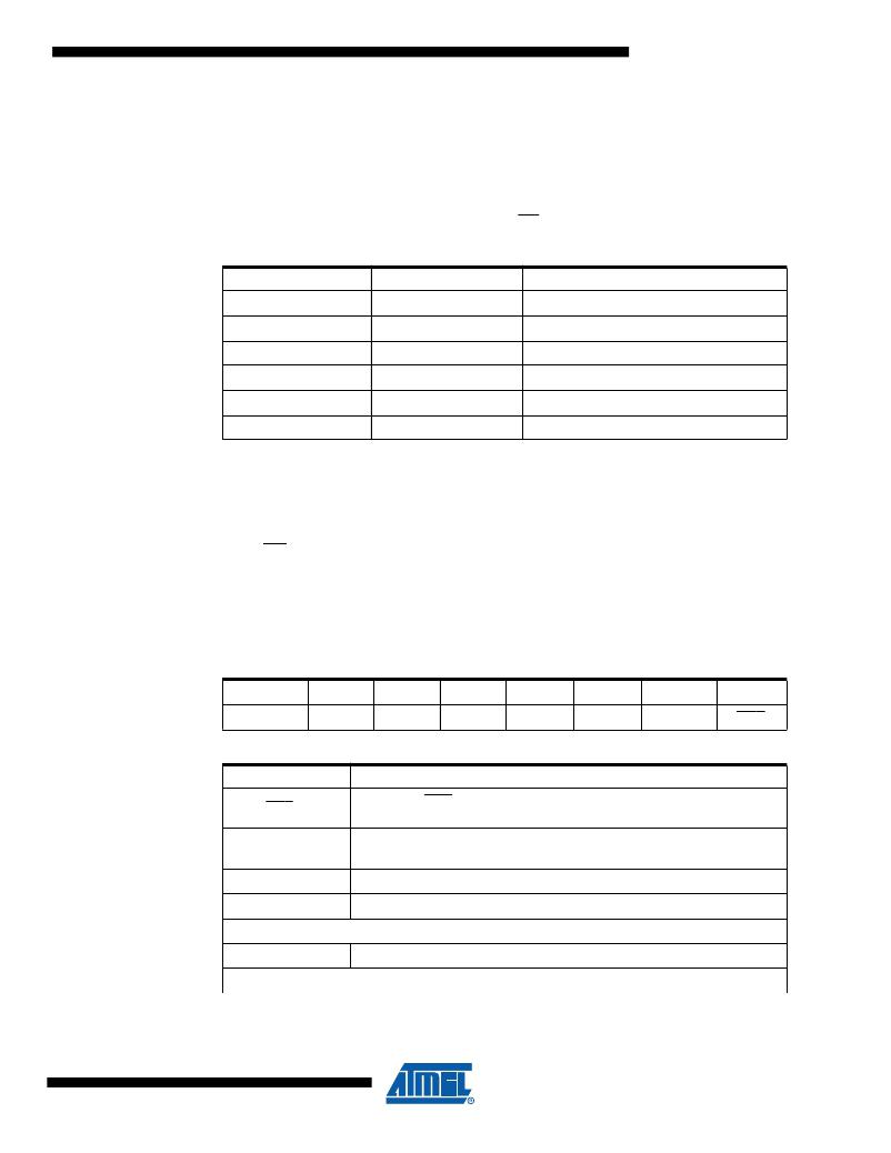
�Table� 3-1.�
�Instruction� Set� for� the� AT25128A/256A�
�Instruction� Name�
�WREN�
�WRDI�
�RDSR�
�WRSR�
�READ�
�WRITE�
�Instruction� Format�
�0000� X110�
�0000� X100�
�0000� X101�
�0000� X001�
�0000� X011�
�0000� X010�
�Operation�
�Set� Write� Enable� Latch�
�Reset� Write� Enable� Latch�
�Read� Status� Register�
�Write� Status� Register�
�Read� Data� from� Memory� Array�
�Write� Data� to� Memory� Array�
�WRITE� ENABLE� (WREN):� The� device� will� power-up� in� the� write� disable� state� when� V� CC� is�
�applied.� All� programming� instructions� must� therefore� be� preceded� by� a� Write� Enable� instruction.�
�WRITE� DISABLE� (WRDI):� To� protect� the� device� against� inadvertent� writes,� the� Write� Disable�
�instruction� disables� all� programming� modes.� The� WRDI� instruction� is� independent� of� the� status�
�of� the� WP� pin.�
�READ� STATUS� REGISTER� (RDSR):� The� Read� Status� Register� instruction� provides� access� to�
�the� status� register.� The� Ready/Busy� and� Write� Enable� status� of� the� device� can� be� determined� by�
�the� RDSR� instruction.� Similarly,� the� Block� Write� Protection� bits� indicate� the� extent� of� protection�
�employed.� These� bits� are� set� by� using� the� WRSR� instruction.�
�Table� 3-2.�
�Status� Register� Format�
�Bit� 7�
�WPEN�
�Bit� 6�
�X�
�Bit� 5�
�X�
�Bit� 4�
�X�
�Bit� 3�
�BP1�
�Bit� 2�
�BP0�
�Bit� 1�
�WEN�
�Bit� 0�
�RDY�
�Table� 3-3.�
�Bit�
�Bit� 0� (RDY)�
�Bit� 1� (WEN)�
�Bit� 2� (BP0)�
�Bit� 3� (BP1)�
�Read� Status� Register� Bit� Definition�
�Definition�
�Bit� 0� =� “0”� (RDY)� indicates� the� device� is� ready.�
�Bit� 0� =� “1”� indicates� the� write� cycle� is� in� progress.�
�Bit� 1� =� 0� indicates� the� device� is� not� write� enabled.� Bit� 1� =� “1”� indicates�
�the� device� is� write� enabled.�
�See� Table� 3-4� on� page� 10� .�
�See� Table� 3-4� on� page� 10� .�
�Bits� 4� ?� 6� are� 0s� when� device� is� not� in� an� internal� write� cycle.�
�Bit� 7� (WPEN)�
�See� Table� 3-5� on� page� 10� .�
�Bits� 0� ?� 7� are� “1”s� during� an� internal� write� cycle.�
�9�
�3368J–SEEPR–06/07�
�相关PDF资料 |
PDF描述 |
|---|---|
| RN-0907S/HP | CONV DC/DC 1.25W 09VIN 07VOUT |
| ECM06DSEI-S13 | CONN EDGECARD 12POS .156 EXTEND |
| RBB13DHLN | CONN EDGECARD 26POS DIP .050 SLD |
| 345-070-542-801 | CARDEDGE 70POS DUAL .100 GREEN |
| R2D-1209/P-R | CONV DC/DC 2W 12VIN +/-09VOUT |
相关代理商/技术参数 |
参数描述 |
|---|---|
| AT25256AW10SU27 SL383 | 制造商:Atmel Corporation 功能描述:SERIAL EEPROM, 256K (32K X 8), |
| AT25256A-W2.7-11 | 制造商:ATMEL 制造商全称:ATMEL Corporation 功能描述:SPI Serial EEPROMs |
| AT25256AY4-10YU-1.8 | 制造商:ATMEL 制造商全称:ATMEL Corporation 功能描述:SPI Serial EEPROMs |
| AT25256B | 制造商:ATMEL 制造商全称:ATMEL Corporation 功能描述:serial electrically-erasable programmable read only memory |
| AT25256B-CUL-T | 制造商:Atmel Corporation 功能描述: 制造商:Atmel Corporation 功能描述:8 DBGA2, PB/HALO FREE, 1.8V - Tape and Reel |
发布紧急采购,3分钟左右您将得到回复。