参数资料
| 型号: | AT28C64B-15PU |
| 厂商: | Atmel |
| 文件页数: | 3/18页 |
| 文件大小: | 0K |
| 描述: | IC EEPROM 64KBIT 150NS 28DIP |
| 标准包装: | 14 |
| 格式 - 存储器: | EEPROMs - 并行 |
| 存储器类型: | EEPROM |
| 存储容量: | 64K (8K x 8) |
| 速度: | 150ns |
| 接口: | 并联 |
| 电源电压: | 4.5 V ~ 5.5 V |
| 工作温度: | -40°C ~ 85°C |
| 封装/外壳: | 28-DIP(0.600",15.24mm) |
| 供应商设备封装: | 28-PDIP |
| 包装: | 管件 |
| 产品目录页面: | 1458 (CN2011-ZH PDF) |
�� �
�
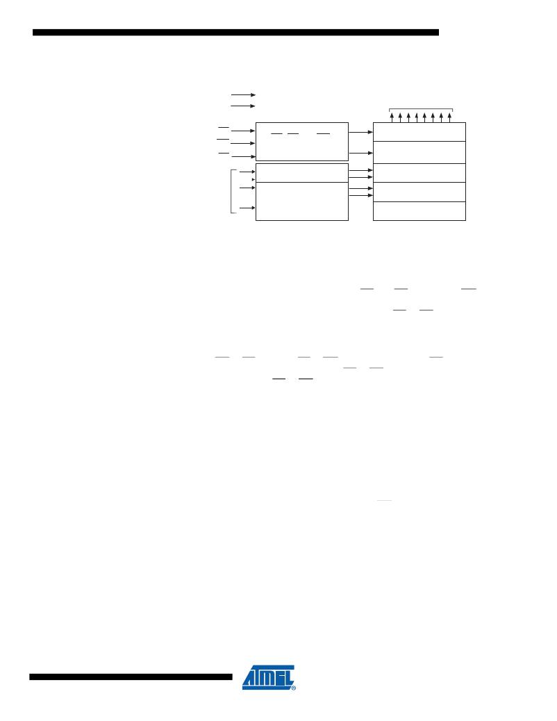
�AT28C64B�
�3.� Block� Diagram�
�VCC�
�GND�
�DATA� INPUTS/OUTPUTS�
�I/O0� -� I/O7�
�OE�
�WE�
�OE,� CE� and� WE�
�LOGIC�
�DATA� LATCH�
�INPUT/OUTPUT�
�CE�
�ADDRESS�
�INPUTS�
�Y� DECODER�
�BUFFERS�
�Y-GATING�
�CELL� MATRIX�
�X� DECODER�
�IDENTIFICATION�
�4.� Device� Operation�
�4.1�
�4.2�
�4.3�
�Read�
�Byte� Write�
�Page� Write�
�The� AT28C64B� is� accessed� like� a� Static� RAM.� When� CE� and� OE� are� low� and� WE� is� high,� the�
�data� stored� at� the� memory� location� determined� by� the� address� pins� is� asserted� on� the� outputs.�
�The� outputs� are� put� in� the� high-impedance� state� when� either� CE� or� OE� is� high.� This� dual� line�
�control� gives� designers� flexibility� in� preventing� bus� contention� in� their� systems.�
�A� low� pulse� on� the� WE� or� CE� input� with� CE� or� WE� low� (respectively)� and� OE� high� initiates� a� write�
�cycle.� The� address� is� latched� on� the� falling� edge� of� CE� or� WE,� whichever� occurs� last.� The� data� is�
�latched� by� the� first� rising� edge� of� CE� or� WE.� Once� a� byte� write� has� been� started,� it� will� automati-�
�cally� time� itself� to� completion.� Once� a� programming� operation� has� been� initiated� and� for� the�
�duration� of� t� WC� ,� a� read� operation� will� effectively� be� a� polling� operation.�
�The� page� write� operation� of� the� AT28C64B� allows� 1� to� 64� bytes� of� data� to� be� written� into� the�
�device� during� a� single� internal� programming� period.� A� page� write� operation� is� initiated� in� the�
�same� manner� as� a� byte� write;� after� the� first� byte� is� written,� it� can� then� be� followed� by� 1� to� 63�
�additional� bytes.� Each� successive� byte� must� be� loaded� within� 150� μs� (t� BLC� )� of� the� previous� byte.�
�If� the� t� BLC� limit� is� exceeded,� the� AT28C64B� will� cease� accepting� data� and� commence� the� internal�
�programming� operation.� All� bytes� during� a� page� write� operation� must� reside� on� the� same� page�
�as� defined� by� the� state� of� the� A6� to� A12� inputs.� For� each� WE� high� to� low� transition� during� the�
�page� write� operation,� A6� to� A12� must� be� the� same.�
�The� A0� to� A5� inputs� specify� which� bytes� within� the� page� are� to� be� written.� The� bytes� may� be�
�loaded� in� any� order� and� may� be� altered� within� the� same� load� period.� Only� bytes� which� are� spec-�
�ified� for� writing� will� be� written;� unnecessary� cycling� of� other� bytes� within� the� page� does� not� occur.�
�3�
�0270L–PEEPR–2/09�
�相关PDF资料 |
PDF描述 |
|---|---|
| AT28C64B-15JU | IC EEPROM 64KBIT 150NS 32PLCC |
| AGLP060V2-VQG176I | IC FPGA IGLOO PLUS 60K 176-VQFN |
| AGLP060V2-VQ176I | IC FPGA IGLOO PLUS 60K 176-VQFN |
| AT28HC64BF-12SU | IC EEPROM 64KBIT 120NS 28SOIC |
| A3P060-1VQ100T | IC FPGA 1KB FLASH 60K 100-VQFP |
相关代理商/技术参数 |
参数描述 |
|---|---|
| AT28C64B-15SA | 功能描述:IC EEPROM 64KBIT 150NS 28SOIC RoHS:否 类别:集成电路 (IC) >> 存储器 系列:- 标准包装:378 系列:- 格式 - 存储器:闪存 存储器类型:FLASH 存储容量:8M(1M x 8,512K x 16) 速度:110ns 接口:并联 电源电压:2.7 V ~ 3.6 V 工作温度:-40°C ~ 85°C 封装/外壳:48-CBGA 供应商设备封装:48-CBGA(7x7) 包装:托盘 |
| AT28C64B-15SC | 功能描述:电可擦除可编程只读存储器 DIE WAFER FORM - 150NS COM TEMP RoHS:否 制造商:Atmel 存储容量:2 Kbit 组织:256 B x 8 数据保留:100 yr 最大时钟频率:1000 KHz 最大工作电流:6 uA 工作电源电压:1.7 V to 5.5 V 最大工作温度:+ 85 C 安装风格:SMD/SMT 封装 / 箱体:SOIC-8 |
| AT28C64B-15SI | 功能描述:电可擦除可编程只读存储器 DIE WAFER FORM - 150NS IND TEMP RoHS:否 制造商:Atmel 存储容量:2 Kbit 组织:256 B x 8 数据保留:100 yr 最大时钟频率:1000 KHz 最大工作电流:6 uA 工作电源电压:1.7 V to 5.5 V 最大工作温度:+ 85 C 安装风格:SMD/SMT 封装 / 箱体:SOIC-8 |
| AT28C64B-15SI SL527 | 制造商:Atmel Corporation 功能描述:QT# WA145434 |
| AT28C64B-15SU | 功能描述:电可擦除可编程只读存储器 64K 8K x 8 150 ns 4.5V-5.5V RoHS:否 制造商:Atmel 存储容量:2 Kbit 组织:256 B x 8 数据保留:100 yr 最大时钟频率:1000 KHz 最大工作电流:6 uA 工作电源电压:1.7 V to 5.5 V 最大工作温度:+ 85 C 安装风格:SMD/SMT 封装 / 箱体:SOIC-8 |
发布紧急采购,3分钟左右您将得到回复。