- 您现在的位置:买卖IC网 > PDF目录381452 > AT45DB011B-XI (ATMEL CORP) 1-MEGABIT 2.7 VOLT ONLY DATA FLASH PDF资料下载
参数资料
| 型号: | AT45DB011B-XI |
| 厂商: | ATMEL CORP |
| 元件分类: | DRAM |
| 英文描述: | 1-MEGABIT 2.7 VOLT ONLY DATA FLASH |
| 中文描述: | 1M X 1 FLASH 2.7V PROM, PDSO14 |
| 封装: | 4.40 MM, PLASTIC, MO-153AB-1, TSSOP-14 |
| 文件页数: | 3/32页 |
| 文件大小: | 319K |
| 代理商: | AT45DB011B-XI |
第1页第2页当前第3页第4页第5页第6页第7页第8页第9页第10页第11页第12页第13页第14页第15页第16页第17页第18页第19页第20页第21页第22页第23页第24页第25页第26页第27页第28页第29页第30页第31页第32页
3
AT45DB011B
1984H–DFLSH–10/04
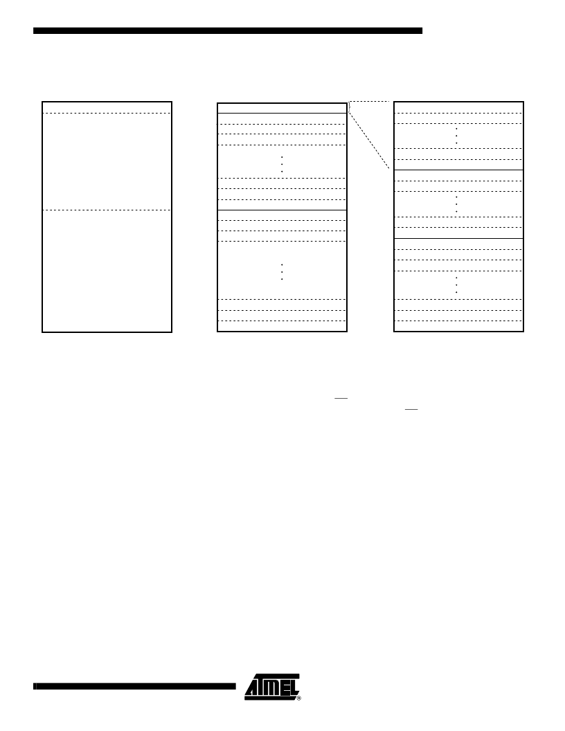
Memory Architecture Diagram
Device
Operation
The device operation is controlled by instructions from the host processor. The list of instruc-
tions and their associated opcodes are contained in Tables 1 through 4 (pages 11 and 12). A
valid instruction starts with the falling edge of CS followed by the appropriate 8-bit opcode and
the desired buffer or main memory address location. While the CS pin is low, toggling the SCK
pin controls the loading of the opcode and the desired buffer or main memory address location
through the SI (serial input) pin. All instructions, addresses, and data are transferred with the
most significant bit (MSB) first.
Buffer addressing is referenced in the datasheet using the terminology BFA8-BFA0 to denote
the nine address bits required to designate a byte address within a buffer. Main memory
addressing is referenced using the terminology PA8-PA0 and BA8-BA0 where PA8-PA0
denotes the 10 address bits required to designate a page address and BA8-BA0 denotes the
nine address bits required to designate a byte address within the page.
Read Commands
By specifying the appropriate opcode, data can be read from the main memory or from the
data buffer. The DataFlash supports two categories of read modes in relation to the SCK sig-
nal. The differences between the modes are in respect to the inactive state of the SCK signal
as well as which clock cycle data will begin to be output. The two categories, which are com-
prised of four modes total, are defined as Inactive Clock Polarity Low or Inactive Clock Polarity
High and SPI Mode 0 or SPI Mode 3. A separate opcode (refer to Table 1 on page 11 for a
complete list) is used to select which category will be used for reading. Please refer to the
“Detailed Bit-level Read Timing” diagrams in this datasheet for details on the clock cycle
sequences for each mode.
Block = 2112 bytes
(2K + 64)
8 Pages
BLOCK 0
BLOCK 1
BLOCK 2
BLOCK 62
BLOCK 63
BLOCK 61
Page = 264 bytes
(256 + 8)
PAGE 0
PAGE 1
PAGE 6
PAGE 7
PAGE 8
PAGE 9
PAGE 510
PAGE 511
B
PAGE 14
PAGE 15
PAGE 16
PAGE 17
PAGE 18
PAGE 509
B
BLOCK ARCHITECTURE
PAGE ARCHITECTURE
SECTOR 0 = 2112 BYTES (2K + 64)
SECTOR 1 = 65,472 BYTES (62K + 1984)
SECTOR ARCHITECTURE
SECTOR 2 = 67,584 BYTES (64K + 2K)
BLOCK 3
BLOCK 29
BLOCK 30
BLOCK 31
BLOCK 32
BLOCK 33
BLOCK 34
S
S
SECTOR 0
相关PDF资料 |
PDF描述 |
|---|---|
| AT45DB011B-XU | 1-MEGABIT 2.7 VOLT ONLY DATA FLASH |
| AT45DB011D | 1-megabit 2.7-volt DataFlash |
| AT45DB011D_07 | 1-megabit 2.7-volt DataFlash |
| AT45DB011D-MU | 1-megabit 2.7-volt DataFlash |
| AT45DB011D-SSU | 1-megabit 2.7-volt DataFlash |
相关代理商/技术参数 |
参数描述 |
|---|---|
| AT45DB011B-XU | 功能描述:闪存 1M SERIAL 2.7V - IND TEMP RoHS:否 制造商:ON Semiconductor 数据总线宽度:1 bit 存储类型:Flash 存储容量:2 MB 结构:256 K x 8 定时类型: 接口类型:SPI 访问时间: 电源电压-最大:3.6 V 电源电压-最小:2.3 V 最大工作电流:15 mA 工作温度:- 40 C to + 85 C 安装风格:SMD/SMT 封装 / 箱体: 封装:Reel |
| AT45DB011D | 制造商:ATMEL 制造商全称:ATMEL Corporation 功能描述:1-megabit 2.7-volt Minimum DataFlash |
| AT45DB011D_07 | 制造商:ATMEL 制造商全称:ATMEL Corporation 功能描述:1-megabit 2.7-volt DataFlash |
| AT45DB011D_08 | 制造商:ATMEL 制造商全称:ATMEL Corporation 功能描述:1-megabit 2.7-volt Minimum DataFlash |
| AT45DB011D_09 | 制造商:ATMEL 制造商全称:ATMEL Corporation 功能描述:1-megabit 2.7-volt Minimum DataFlash |
发布紧急采购,3分钟左右您将得到回复。