- 您现在的位置:买卖IC网 > PDF目录381453 > AT45DB041D-MU (ATMEL CORP) 4-megabit 2.5-volt or 2.7-volt DataFlash PDF资料下载
参数资料
| 型号: | AT45DB041D-MU |
| 厂商: | ATMEL CORP |
| 元件分类: | DRAM |
| 英文描述: | 4-megabit 2.5-volt or 2.7-volt DataFlash |
| 中文描述: | 4M X 1 FLASH 2.7V PROM, DSO8 |
| 封装: | 6 X 5 MM, 0.60 MM HEIGHT, GREEN, PLASTIC, MO-229, MLF-8 |
| 文件页数: | 10/53页 |
| 文件大小: | 1085K |
| 代理商: | AT45DB041D-MU |
第1页第2页第3页第4页第5页第6页第7页第8页第9页当前第10页第11页第12页第13页第14页第15页第16页第17页第18页第19页第20页第21页第22页第23页第24页第25页第26页第27页第28页第29页第30页第31页第32页第33页第34页第35页第36页第37页第38页第39页第40页第41页第42页第43页第44页第45页第46页第47页第48页第49页第50页第51页第52页第53页
10
3595H–DFLASH–03/07
AT45DB041D
7.7
Chip Erase
(1)
The entire main memory can be erased at one time by using the Chip Erase command.
To execute the Chip Erase command, a 4-byte command sequence C7H, 94H, 80H and 9AH
must be clocked into the device. Since the entire memory array is to be erased, no address
bytes need to be clocked into the device, and any data clocked in after the opcode will be
ignored. After the last bit of the opcode sequence has been clocked in, the CS pin can be deas-
serted to start the erase process. The erase operation is internally self-timed and should take
place in a time of t
CE
. During this time, the Status Register will indicate that the device is busy.
The Chip Erase command will not affect sectors that are protected or locked down; the contents
of those sectors will remain unchanged. Only those sectors that are not protected or locked
down will be erased.
The WP pin can be asserted while the device is erasing, but protection will not be activated until
the internal erase cycle completes.
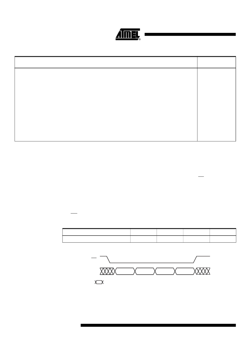
Figure 7-1.
Chip Erase
Note:
1. Refer to the errata regarding Chip Erase on
page 52
.
Table 7-2.
Sector Erase Addressing
PA10/
A18
PA9/
A17
PA8/
A16
PA7/
A15
PA6/
A14
PA5/
A13
PA4/
A12
PA3/
A11
PA2/
A10
PA1/
A9
PA0/
A8
Sector
0
0
0
0
0
0
0
0
X
X
X
0a
0
0
0
0
0
0
0
1
X
X
X
0b
0
0
1
X
X
X
X
X
X
X
X
1
0
1
0
X
X
X
X
X
X
X
X
2
1
0
0
X
X
X
X
X
X
X
X
4
1
0
1
X
X
X
X
X
X
X
X
5
1
1
0
X
X
X
X
X
X
X
X
6
1
1
1
X
X
X
X
X
X
X
X
7
Command
Byte 1
Byte 2
Byte 3
Byte 4
Chip Erase
C7H
94H
80H
9AH
Opcode
Byte 1
Opcode
Byte 2
Opcode
Byte 3
Opcode
Byte 4
CS
Each transition
represents 8 bits
SI
相关PDF资料 |
PDF描述 |
|---|---|
| AT45DB041D-MU-2.5 | 4-megabit 2.5-volt or 2.7-volt DataFlash |
| AT45DB041D-SSU | 4-megabit 2.5-volt or 2.7-volt DataFlash |
| AT45DB041D-SSU-2.5 | 4-megabit 2.5-volt or 2.7-volt DataFlash |
| AT45DB041D-SU | 4-megabit 2.5-volt or 2.7-volt DataFlash |
| AT45DB041D-SU-2.5 | 4-megabit 2.5-volt or 2.7-volt DataFlash |
相关代理商/技术参数 |
参数描述 |
|---|---|
| AT45DB041D-MU-2.5 | 功能描述:闪存 4MB SERIAL 2.5V - IND TEMP RoHS:否 制造商:ON Semiconductor 数据总线宽度:1 bit 存储类型:Flash 存储容量:2 MB 结构:256 K x 8 定时类型: 接口类型:SPI 访问时间: 电源电压-最大:3.6 V 电源电压-最小:2.3 V 最大工作电流:15 mA 工作温度:- 40 C to + 85 C 安装风格:SMD/SMT 封装 / 箱体: 封装:Reel |
| AT45DB041D-MU-2.5-SL383 | 制造商:Adesto Technologies Corporation 功能描述:8-VDFN (5X6), IND TEMP, 2.5V, T&R - Tape and Reel 制造商:Adesto Technologies Corporation 功能描述:IC FLASH 4MBIT 50MHZ 8VDFN 制造商:Adesto Technologies Corporation 功能描述:Flash 4M, 66MHz 2.5-3.6V DataFlash |
| AT45DB041D-MUHT-T | 制造商:Adesto Technologies Corporation 功能描述:8-UDFN (5X6), EXT TEMP NON-AECQ 2.7V T&R - Tape and Reel |
| AT45DB041D-MU-SL383 | 制造商:Adesto Technologies Corporation 功能描述:8-VDFN (5X6), IND TEMP, 2.7V, T&R - Tape and Reel 制造商:Adesto Technologies Corporation 功能描述:IC FLASH 4MBIT 66MHZ 8VDFN 制造商:Adesto Technologies Corporation 功能描述:Flash 4M, 66MHz 2.7-3.6V DataFlash |
| AT45DB041D-MU-SL954 | 制造商:Adesto Technologies Corporation 功能描述:IC FLASH 4MBIT 66MHZ 8VDFN |
发布紧急采购,3分钟左右您将得到回复。