- 您现在的位置:买卖IC网 > PDF目录381473 > AT49F040A-70TI (ATMEL CORP) 4-megabit (512K x 8) 5-volt Only Flash Memory PDF资料下载
参数资料
| 型号: | AT49F040A-70TI |
| 厂商: | ATMEL CORP |
| 元件分类: | DRAM |
| 英文描述: | 4-megabit (512K x 8) 5-volt Only Flash Memory |
| 中文描述: | 512K X 8 FLASH 5V PROM, 70 ns, PDSO32 |
| 封装: | 8 X 20 MM, PLASTIC, MO-142BD, TSOP1-32 |
| 文件页数: | 5/16页 |
| 文件大小: | 248K |
| 代理商: | AT49F040A-70TI |
5
AT49F040A
3359B–FLASH–10/04
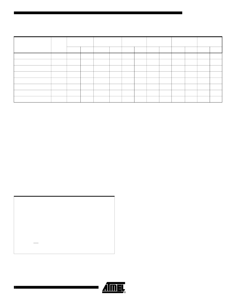
Notes:
1. The DATA FORMAT in each bus cycle is as follows: I/O7 - I/O0 (Hex). The address format in each bus cycle is as follows:
A11 - A0 (Hex); A11 - A18 (don’t care).
2. Since A11 is don’t care, AAA can be replaced with 2AA.
3. The 16K byte boot sector has the address range 00000H to 03FFFH.
4. Either one of the Product ID Exit commands can be used.
5. SA = sector addresses:
SA = 00000 to 03FFF for BOOT BLOCK
SA = 04000 to 05FFF for PARAMETER BLOCK 1
SA = 06000 to 07FFF for PARAMETER BLOCK 2
SA = 08000 to FFFF for MAIN MEMORY ARRAY BLOCK 1
SA = 10000 to 1FFFF for MAIN MEMORY ARRAY BLOCK 2
SA = 20000 to 2FFFF for MAIN MEMORY ARRAY BLOCK 3
SA = 30000 to 3FFFF for MAIN MEMORY ARRAY BLOCK 4
SA = 40000 to 4FFFF for MAIN MEMORY ARRAY BLOCK 5
SA = 50000 to 5FFFF for MAIN MEMORY ARRAY BLOCK 6
SA = 60000 to 6FFFF for MAIN MEMORY ARRAY BLOCK 7
SA = 70000 to 7FFFF for MAIN MEMORY ARRAY BLOCK 8
Command Definition (in Hex)
(1)
Command
Sequence
Bus
Cycles
1st Bus
Cycle
2nd Bus
Cycle
3rd Bus
Cycle
4th Bus
Cycle
5th Bus
Cycle
6th Bus
Cycle
Addr
Data
Addr
Data
Addr
Data
Addr
Data
Addr
Data
Addr
Data
Read
1
Addr
D
OUT
Chip Erase
6
555
AA
AAA
(2)
55
555
80
555
AA
AAA
55
555
10
Sector Erase
6
555
AA
AAA
55
555
80
555
AA
AAA
55
SA
(5)
30
Byte Program
4
555
AA
AAA
55
555
A0
Addr
D
IN
Boot Block Lockout
(3)
6
555
AA
AAA
55
555
80
555
AA
AAA
55
555
40
Product ID Entry
3
555
AA
AAA
55
555
90
Product ID Exit
(4)
3
555
AA
AAA
55
555
F0
Product ID Exit
(4)
1
XXXX
F0
Absolute Maximum Ratings*
Temperature Under Bias................................ -55°C to +125°C
*NOTICE:
Stresses beyond those listed under “Absolute Maxi-
mum Ratings” may cause permanent damage to the
device. This is a stress rating only and functional
operation of the device at these or any other condi-
tions beyond those indicated in the operational sec-
tions of this specification is not implied. Exposure to
absolute maximum rating conditions for extended
periods may affect device reliability.
Storage Temperature..................................... -65°C to +150°C
All Input Voltages
(including NC Pins)
with Respect to Ground...................................-0.6V to +6.25V
All Output Voltages
with Respect to Ground.............................-0.6V to V
CC
+ 0.6V
Voltage on OE
with Respect to Ground...................................-0.6V to +13.5V
相关PDF资料 |
PDF描述 |
|---|---|
| AT49F080T-12CC | 8-Megabit 1M x 8 5-volt Only Flash Memory |
| AT49F080T-12CI | 8-Megabit 1M x 8 5-volt Only Flash Memory |
| AT49F080T-12RC | 8-Megabit 1M x 8 5-volt Only Flash Memory |
| AT49F080T-12RI | 8-Megabit 1M x 8 5-volt Only Flash Memory |
| AT49F080T-12TC | 8-Megabit 1M x 8 5-volt Only Flash Memory |
相关代理商/技术参数 |
参数描述 |
|---|---|
| AT49F040A-70TI SL383 | 功能描述:IC FLASH 4MBIT 70NS 32TSOP RoHS:否 类别:集成电路 (IC) >> 存储器 系列:- 标准包装:1 系列:- 格式 - 存储器:RAM 存储器类型:SDRAM 存储容量:256M(8Mx32) 速度:143MHz 接口:并联 电源电压:3 V ~ 3.6 V 工作温度:-40°C ~ 85°C 封装/外壳:90-VFBGA 供应商设备封装:90-VFBGA(8x13) 包装:托盘 其它名称:Q2841869 |
| AT49F040A-70TI-T | 功能描述:IC FLASH 4MBIT 70NS 32TSOP 制造商:microchip technology 系列:- 包装:带卷(TR) 零件状态:停產 存储器类型:非易失 存储器格式:闪存 技术:FLASH 存储容量:4Mb (512K x 8) 写周期时间 - 字,页:40μs 访问时间:70ns 存储器接口:并联 电压 - 电源:4.5 V ~ 5.5 V 工作温度:-40°C ~ 85°C(TC) 安装类型:表面贴装 封装/外壳:32-TFSOP(0.724",18.40mm 宽) 供应商器件封装:32-TSOP 基本零件编号:AT49F040 标准包装:1,500 |
| AT49F040A-70TU | 功能描述:IC FLASH 4MBIT 70NS 32TSOP RoHS:是 类别:集成电路 (IC) >> 存储器 系列:- 标准包装:1 系列:- 格式 - 存储器:RAM 存储器类型:SDRAM 存储容量:256M(8Mx32) 速度:143MHz 接口:并联 电源电压:3 V ~ 3.6 V 工作温度:-40°C ~ 85°C 封装/外壳:90-VFBGA 供应商设备封装:90-VFBGA(8x13) 包装:托盘 其它名称:Q2841869 |
| AT49F040A-70TU SL383 | 功能描述:IC FLASH 4MBIT 70NS 32TSOP RoHS:是 类别:集成电路 (IC) >> 存储器 系列:- 标准包装:1 系列:- 格式 - 存储器:RAM 存储器类型:SDRAM 存储容量:256M(8Mx32) 速度:143MHz 接口:并联 电源电压:3 V ~ 3.6 V 工作温度:-40°C ~ 85°C 封装/外壳:90-VFBGA 供应商设备封装:90-VFBGA(8x13) 包装:托盘 其它名称:Q2841869 |
| AT49F040A-70TU-T | 功能描述:IC FLASH 4MBIT 70NS 32TSOP 制造商:microchip technology 系列:- 包装:带卷(TR) 零件状态:停產 存储器类型:非易失 存储器格式:闪存 技术:FLASH 存储容量:4Mb (512K x 8) 写周期时间 - 字,页:40μs 访问时间:70ns 存储器接口:并联 电压 - 电源:4.5 V ~ 5.5 V 工作温度:-40°C ~ 85°C(TC) 安装类型:表面贴装 封装/外壳:32-TFSOP(0.724",18.40mm 宽) 供应商器件封装:32-TSOP 基本零件编号:AT49F040 标准包装:1,500 |
发布紧急采购,3分钟左右您将得到回复。