- 您现在的位置:买卖IC网 > PDF目录11216 > AT89C4051-24PU (Atmel)IC MCU 4K FLASH 24MHZ 20-DIP PDF资料下载
参数资料
| 型号: | AT89C4051-24PU |
| 厂商: | Atmel |
| 文件页数: | 19/19页 |
| 文件大小: | 0K |
| 描述: | IC MCU 4K FLASH 24MHZ 20-DIP |
| 产品培训模块: | MCU Product Line Introduction |
| 标准包装: | 18 |
| 系列: | 89C |
| 核心处理器: | 8051 |
| 芯体尺寸: | 8-位 |
| 速度: | 24MHz |
| 连通性: | UART/USART |
| 外围设备: | 欠压检测/复位,LED,POR |
| 输入/输出数: | 15 |
| 程序存储器容量: | 4KB(4K x 8) |
| 程序存储器类型: | 闪存 |
| RAM 容量: | 128 x 8 |
| 电压 - 电源 (Vcc/Vdd): | 4 V ~ 6 V |
| 振荡器型: | 内部 |
| 工作温度: | -40°C ~ 85°C |
| 封装/外壳: | 20-DIP(0.300",7.62mm) |
| 包装: | 管件 |
9
1001F–MICRO–6/08
AT89C4051
Program Verify: If lock bits LB1 and LB2 have not been programmed code data can be read
back via the data lines for verification:
1.
Reset the internal address counter to 000H by bringing RST from “L” to “H”.
2.
Apply the appropriate control signals for Read Code data and read the output data at
the port P1 pins.
3.
Pulse pin XTAL1 once to advance the internal address counter.
4.
Read the next code data byte at the port P1 pins.
5.
Repeat steps 3 and 4 until the entire array is read.
The lock bits cannot be verified directly. Verification of the lock bits is achieved by observing that
their features are enabled.
Chip Erase: The entire PEROM array (4K bytes) and the two Lock Bits are erased electrically
by using the proper combination of control signals and by holding P3.2 low for 10 ms. The code
array is written with all “1”s in the Chip Erase operation and must be executed before any non-
blank memory byte can be re-programmed.
Reading the Signature Bytes: The signature bytes are read by the same procedure as a nor-
mal verification of locations 000H, 001H, and 002H, except that P3.5 and P3.7 must be pulled to
a logic low. The values returned are as follows.
(000H) = 1EH indicates manufactured by Atmel
(001H) = 41H indicates AT89C4051
13. Programming Interface
Every code byte in the Flash array can be written and the entire array can be erased by using
the appropriate combination of control signals. The write operation cycle is self-timed and once
initiated, will automatically time itself to completion.
Most major worldwide programming vendors offer support for the Atmel AT89 microcontroller
series. Please contact your local programming vendor for the appropriate software revision.
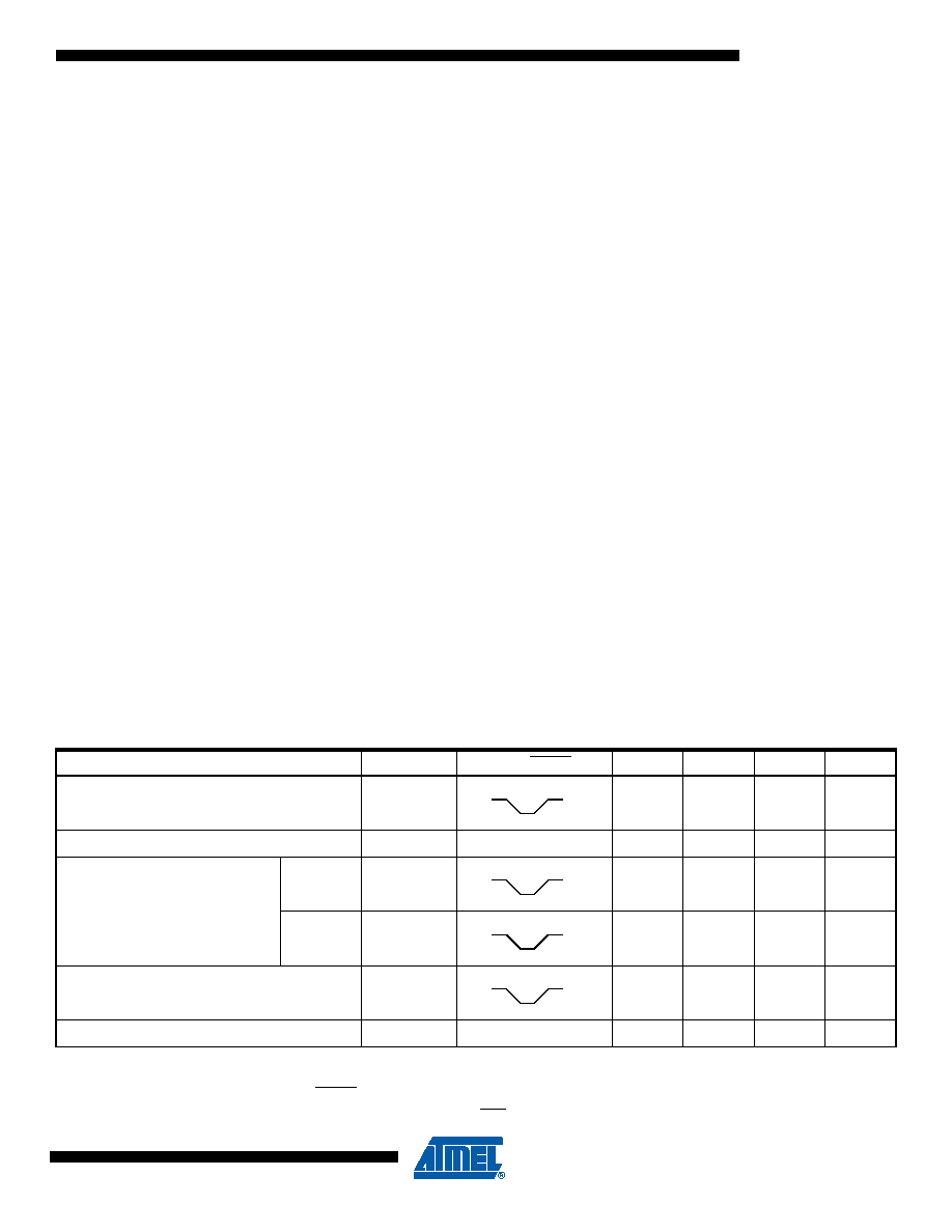
Notes:
1. The internal PEROM address counter is reset to 000H on the rising edge of RST and is advanced by a positive pulse at
XTAL1 pin.
2. Chip Erase requires a 10-ms PROG pulse.
3. P3.1 is pulled Low during programming to indicate RDY/BSY.
13.1
Flash Programming Modes
Mode
RST/V
PP
P3.2/PROG
P3.3
P3.4
P3.5
P3.7
Write Code Data(1)(3)
12V
L
H
Read Code Data(1)
HH
L
H
Write Lock
Bit - 1
12V
HH
Bit - 2
12V
H
L
Chip Erase
12V
H
L
Read Signature Byte
H
L
(2)
相关PDF资料 |
PDF描述 |
|---|---|
| VE-B30-IX-F3 | CONVERTER MOD DC/DC 5V 75W |
| ADG731BCPZ-REEL | IC MULTIPLEXER 32X1 48LFCSP |
| ADG201HSKPZ-REEL | IC SWITCH QUAD SPST 20PLCC |
| ADG707BRU | IC MULTIPLEXER DUAL 8X1 28TSSOP |
| ADG706BRU | IC MULTIPLEXER 16X1 28TSSOP |
相关代理商/技术参数 |
参数描述 |
|---|---|
| AT89C4051-24PU SL383 | 制造商:Atmel Corporation 功能描述:8051 4K FLASH 2.7 TO 5.5V, PDI |
| AT89C4051-24SC | 功能描述:8位微控制器 -MCU 4K FLASH 2.7 TO 5.5V 24MHZ COM TEMP RoHS:否 制造商:Silicon Labs 核心:8051 处理器系列:C8051F39x 数据总线宽度:8 bit 最大时钟频率:50 MHz 程序存储器大小:16 KB 数据 RAM 大小:1 KB 片上 ADC:Yes 工作电源电压:1.8 V to 3.6 V 工作温度范围:- 40 C to + 105 C 封装 / 箱体:QFN-20 安装风格:SMD/SMT |
| AT89C4051-24SI | 功能描述:8位微控制器 -MCU 4K FLASH 2.7 TO 5.5V 24MHZ IND TEMP RoHS:否 制造商:Silicon Labs 核心:8051 处理器系列:C8051F39x 数据总线宽度:8 bit 最大时钟频率:50 MHz 程序存储器大小:16 KB 数据 RAM 大小:1 KB 片上 ADC:Yes 工作电源电压:1.8 V to 3.6 V 工作温度范围:- 40 C to + 105 C 封装 / 箱体:QFN-20 安装风格:SMD/SMT |
| AT89C4051-24SJ | 功能描述:8位微控制器 -MCU Microcontroller RoHS:否 制造商:Silicon Labs 核心:8051 处理器系列:C8051F39x 数据总线宽度:8 bit 最大时钟频率:50 MHz 程序存储器大小:16 KB 数据 RAM 大小:1 KB 片上 ADC:Yes 工作电源电压:1.8 V to 3.6 V 工作温度范围:- 40 C to + 105 C 封装 / 箱体:QFN-20 安装风格:SMD/SMT |
| AT89C4051-24SU | 功能描述:8位微控制器 -MCU 8051 4K FLASH 2.7 TO 5.5V 24MHZ 4V-5.5V RoHS:否 制造商:Silicon Labs 核心:8051 处理器系列:C8051F39x 数据总线宽度:8 bit 最大时钟频率:50 MHz 程序存储器大小:16 KB 数据 RAM 大小:1 KB 片上 ADC:Yes 工作电源电压:1.8 V to 3.6 V 工作温度范围:- 40 C to + 105 C 封装 / 箱体:QFN-20 安装风格:SMD/SMT |
发布紧急采购,3分钟左右您将得到回复。