参数资料
| 型号: | AT89C51AC3-RDTIM |
| 厂商: | Atmel |
| 文件页数: | 101/140页 |
| 文件大小: | 0K |
| 描述: | IC 8051 MCU FLASH 64K 64VQFP |
| 标准包装: | 160 |
| 系列: | 89C |
| 核心处理器: | 8051 |
| 芯体尺寸: | 8-位 |
| 速度: | 60MHz |
| 连通性: | SPI,UART/USART |
| 外围设备: | POR,PWM,WDT |
| 输入/输出数: | 36 |
| 程序存储器容量: | 64KB(64K x 8) |
| 程序存储器类型: | 闪存 |
| EEPROM 大小: | 2K x 8 |
| RAM 容量: | 2.25K x 8 |
| 电压 - 电源 (Vcc/Vdd): | 3 V ~ 5.5 V |
| 数据转换器: | A/D 8x10b |
| 振荡器型: | 外部 |
| 工作温度: | -40°C ~ 85°C |
| 封装/外壳: | 64-LQFP |
| 包装: | 托盘 |
第1页第2页第3页第4页第5页第6页第7页第8页第9页第10页第11页第12页第13页第14页第15页第16页第17页第18页第19页第20页第21页第22页第23页第24页第25页第26页第27页第28页第29页第30页第31页第32页第33页第34页第35页第36页第37页第38页第39页第40页第41页第42页第43页第44页第45页第46页第47页第48页第49页第50页第51页第52页第53页第54页第55页第56页第57页第58页第59页第60页第61页第62页第63页第64页第65页第66页第67页第68页第69页第70页第71页第72页第73页第74页第75页第76页第77页第78页第79页第80页第81页第82页第83页第84页第85页第86页第87页第88页第89页第90页第91页第92页第93页第94页第95页第96页第97页第98页第99页第100页当前第101页第102页第103页第104页第105页第106页第107页第108页第109页第110页第111页第112页第113页第114页第115页第116页第117页第118页第119页第120页第121页第122页第123页第124页第125页第126页第127页第128页第129页第130页第131页第132页第133页第134页第135页第136页第137页第138页第139页第140页
2009 Microchip Technology Inc.
DS70286C-page 61
dsPIC33FJXXXGPX06/X08/X10
4.2.7
SOFTWARE STACK
In addition to its use as a working register, the W15
register in the dsPIC33FJXXXGPX06/X08/X10 devices
is also used as a software Stack Pointer. The Stack
Pointer always points to the first available free word
and grows from lower to higher addresses. It
pre-decrements for stack pops and post-increments for
stack pushes, as shown in Figure 4-6. For a PC push
during any CALL instruction, the MSb of the PC is
zero-extended before the push, ensuring that the MSb
is always clear.
The Stack Pointer Limit register (SPLIM) associated
with the Stack Pointer sets an upper address boundary
for the stack. SPLIM is uninitialized at Reset. As is the
case for the Stack Pointer, SPLIM<0> is forced to ‘0’
because all stack operations must be word-aligned.
Whenever an EA is generated using W15 as a source
or destination pointer, the resulting address is
compared with the value in SPLIM. If the contents of
the Stack Pointer (W15) and the SPLIM register are
equal and a push operation is performed, a stack error
trap will not occur. The stack error trap will occur on a
subsequent push operation. Thus, for example, if it is
desirable to cause a stack error trap when the stack
grows beyond address 0x2000 in RAM, initialize the
SPLIM with the value 0x1FFE.
Similarly, a Stack Pointer underflow (stack error) trap is
generated when the Stack Pointer address is found to
be less than 0x0800. This prevents the stack from
interfering with the Special Function Register (SFR)
space.
A write to the SPLIM register should not be immediately
followed by an indirect read operation using W15.
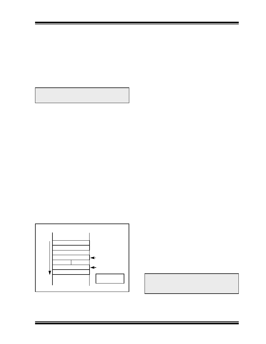
FIGURE 4-6:
CALL
STACK FRAME
4.2.8
DATA RAM PROTECTION FEATURE
The dsPIC33F product family supports Data RAM
protection features which enable segments of RAM to
be protected when used in conjunction with Boot and
Secure Code Segment Security. BSRAM (Secure RAM
segment for BS) is accessible only from the Boot
Segment Flash code when enabled. SSRAM (Secure
RAM segment for RAM) is accessible only from the
Secure Segment Flash code when enabled. See
Table 4-1 for an overview of the BSRAM and SSRAM
SFRs.
4.3
Instruction Addressing Modes
The addressing modes in Table 4-35 form the basis of
the addressing modes optimized to support the specific
features of individual instructions. The addressing
modes provided in the MAC class of instructions are
somewhat different from those in the other instruction
types.
4.3.1
FILE REGISTER INSTRUCTIONS
Most file register instructions use a 13-bit address field
(f) to directly address data present in the first 8192
bytes of data memory (Near Data Space). Most file
register instructions employ a working register, W0,
which is denoted as WREG in these instructions. The
destination is typically either the same file register or
WREG (with the exception of the MUL instruction),
which writes the result to a register or register pair. The
MOV
instruction allows additional flexibility and can
access the entire data space.
4.3.2
MCU INSTRUCTIONS
The 3-operand MCU instructions are of the form:
Operand 3 = Operand 1 <function> Operand 2
where Operand 1 is always a working register (i.e., the
addressing mode can only be register direct) which is
referred to as Wb. Operand 2 can be a W register,
fetched from data memory, or a 5-bit literal. The result
location can be either a W register or a data memory
location. The following addressing modes are
supported by MCU instructions:
Register Direct
Register Indirect
Register Indirect Post-Modified
Register Indirect Pre-Modified
5-bit or 10-bit Literal
Note:
A PC push during exception processing
concatenates the SRL register to the MSb
of the PC prior to the push.
<Free Word>
PC<15:0>
000000000
0
15
W15 (before CALL)
W15 (after CALL)
S
tac
kGr
ows
To
w
ar
ds
Hi
gh
er
Add
re
ss
0x0000
PC<22:16>
POP
: [--W15]
PUSH : [W15++]
Note:
Not all instructions support all the
addressing modes given above. Individual
instructions may support different subsets
of these addressing modes.
相关PDF资料 |
PDF描述 |
|---|---|
| PIC16F84-04/P | IC MCU FLASH 1KX14 EE 18DIP |
| PIC24HJ128GP202-I/SO | IC PIC MCU FLASH 128K 28SOIC |
| PIC24FJ128GA310-I/PT | MCU 16BIT 128KB FLASH 100TQFP |
| DSPIC33FJ16GS504-I/PT | IC DSPIC MCU/DSP 16K 44-TQFP |
| DSPIC33FJ64GP802-I/SO | IC DSPIC MCU/DSP 64K 28-SOIC |
相关代理商/技术参数 |
参数描述 |
|---|---|
| AT89C51AC3-RDTUM | 功能描述:8位微控制器 -MCU C51AC3 64K FLASHADC EEP 5V RoHS:否 制造商:Silicon Labs 核心:8051 处理器系列:C8051F39x 数据总线宽度:8 bit 最大时钟频率:50 MHz 程序存储器大小:16 KB 数据 RAM 大小:1 KB 片上 ADC:Yes 工作电源电压:1.8 V to 3.6 V 工作温度范围:- 40 C to + 105 C 封装 / 箱体:QFN-20 安装风格:SMD/SMT |
| AT89C51AC3-RLTIM | 功能描述:IC 8051 MCU FLASH 64K 44VQFP RoHS:否 类别:集成电路 (IC) >> 嵌入式 - 微控制器, 系列:89C 标准包装:1,500 系列:AVR® ATtiny 核心处理器:AVR 芯体尺寸:8-位 速度:16MHz 连通性:I²C,LIN,SPI,UART/USART,USI 外围设备:欠压检测/复位,POR,PWM,温度传感器,WDT 输入/输出数:16 程序存储器容量:8KB(4K x 16) 程序存储器类型:闪存 EEPROM 大小:512 x 8 RAM 容量:512 x 8 电压 - 电源 (Vcc/Vdd):2.7 V ~ 5.5 V 数据转换器:A/D 11x10b 振荡器型:内部 工作温度:-40°C ~ 125°C 封装/外壳:20-SOIC(0.295",7.50mm 宽) 包装:带卷 (TR) |
| AT89C51AC3-RLTUM | 功能描述:8位微控制器 -MCU C51AC3 64K FLASHADC EEP 5V RoHS:否 制造商:Silicon Labs 核心:8051 处理器系列:C8051F39x 数据总线宽度:8 bit 最大时钟频率:50 MHz 程序存储器大小:16 KB 数据 RAM 大小:1 KB 片上 ADC:Yes 工作电源电压:1.8 V to 3.6 V 工作温度范围:- 40 C to + 105 C 封装 / 箱体:QFN-20 安装风格:SMD/SMT |
| AT89C51AC3-S3SIM | 制造商:ATMEL 制造商全称:ATMEL Corporation 功能描述:Enhanced 8-bit Microcontroller with 64KB Flash Memory |
| AT89C51AC3-S3SUM | 功能描述:8位微控制器 -MCU 64K FLASHADC EEP ind 5V RoHS:否 制造商:Silicon Labs 核心:8051 处理器系列:C8051F39x 数据总线宽度:8 bit 最大时钟频率:50 MHz 程序存储器大小:16 KB 数据 RAM 大小:1 KB 片上 ADC:Yes 工作电源电压:1.8 V to 3.6 V 工作温度范围:- 40 C to + 105 C 封装 / 箱体:QFN-20 安装风格:SMD/SMT |
发布紧急采购,3分钟左右您将得到回复。