参数资料
| 型号: | AT89C51RC2-3CSIM |
| 厂商: | Atmel |
| 文件页数: | 44/127页 |
| 文件大小: | 0K |
| 描述: | IC 8051 MCU FLASH 32K 40DIP |
| 标准包装: | 9 |
| 系列: | 89C |
| 核心处理器: | 8051 |
| 芯体尺寸: | 8-位 |
| 速度: | 60MHz |
| 连通性: | SPI,UART/USART |
| 外围设备: | POR,PWM,WDT |
| 输入/输出数: | 32 |
| 程序存储器容量: | 32KB(32K x 8) |
| 程序存储器类型: | 闪存 |
| RAM 容量: | 1.25K x 8 |
| 电压 - 电源 (Vcc/Vdd): | 2.7 V ~ 5.5 V |
| 振荡器型: | 外部 |
| 工作温度: | -40°C ~ 85°C |
| 封装/外壳: | 40-DIP(0.600",15.24mm) |
| 包装: | 管件 |
| 配用: | AT89STK-11-ND - KIT STARTER FOR AT89C51RX2 |
第1页第2页第3页第4页第5页第6页第7页第8页第9页第10页第11页第12页第13页第14页第15页第16页第17页第18页第19页第20页第21页第22页第23页第24页第25页第26页第27页第28页第29页第30页第31页第32页第33页第34页第35页第36页第37页第38页第39页第40页第41页第42页第43页当前第44页第45页第46页第47页第48页第49页第50页第51页第52页第53页第54页第55页第56页第57页第58页第59页第60页第61页第62页第63页第64页第65页第66页第67页第68页第69页第70页第71页第72页第73页第74页第75页第76页第77页第78页第79页第80页第81页第82页第83页第84页第85页第86页第87页第88页第89页第90页第91页第92页第93页第94页第95页第96页第97页第98页第99页第100页第101页第102页第103页第104页第105页第106页第107页第108页第109页第110页第111页第112页第113页第114页第115页第116页第117页第118页第119页第120页第121页第122页第123页第124页第125页第126页第127页
23
AT89C51RB2/RC2
4180E–8051–10/06
Expanded RAM
(XRAM)
The AT89C51RB2/RC2 provides additional bytes of random access memory (RAM)
space for increased data parameter handling and high-level language usage.
AT89C51RB2/RC2 devices have expanded RAM in external data space; maximum size
and location are described in Table 18.
Table 18. Expanded RAM
The AT89C51RB2/RC2 has internal data memory that is mapped into four separate
segments.
The four segments are:
1.
The Lower 128 Bytes of RAM (addresses 00h to 7Fh) are directly and indirectly
addressable.
2.
The Upper 128 Bytes of RAM (addresses 80h to FFh) are indirectly addressable
only.
3.
The Special Function Registers, SFRs, (addresses 80h to FFh) are directly
addressable only.
4.
The expanded RAM Bytes are indirectly accessed by MOVX instructions, and
with the EXTRAM bit cleared in the AUXR register (see Table 18).
The lower 128 Bytes can be accessed by either direct or indirect addressing. The Upper
128 Bytes can be accessed by indirect addressing only. The Upper 128 Bytes occupy
the same address space as the SFR. That means they have the same address, but are
physically separate from SFR space.
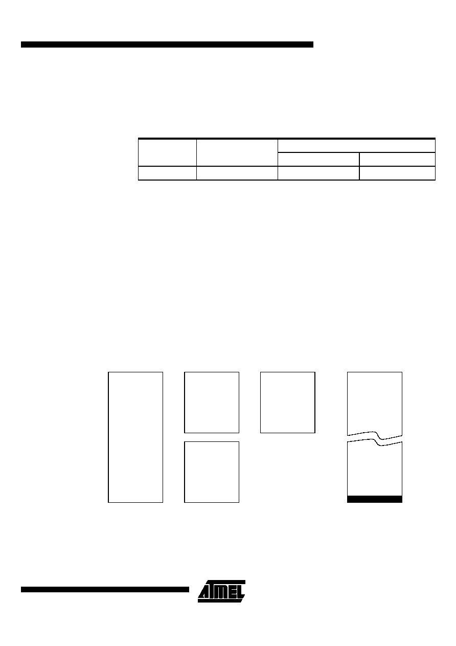
Figure 8. Internal and External Data Memory Address
When an instruction accesses an internal location above address 7Fh, the CPU knows
whether the access is to the upper 128 Bytes of data RAM or to SFR space by the
addressing mode used in the instruction.
Instructions that use direct addressing access SFR space. For example:
MOV 0A0H, # data, accesses the SFR at location 0A0h (which is P2).
Part Number
XRAM Size
Address
Start
End
AT89C51RB2/RC2
1024
00h
3FFh
XRAM
Upper
128 Bytes
Internal
RAM
Lower
128 Bytes
Internal
RAM
Special
Function
Register
80h
00
0FFh or 3FFh
0FFh
00
0FFh
External
Data
Memory
0000
00FFh up to 03FFh
0FFFFh
Indirect Accesses
Direct Accesses
Direct or Indirect
Accesses
7Fh
相关PDF资料 |
PDF描述 |
|---|---|
| AT89C51RB2-SLSIM | IC 8051 MCU FLASH 16K 44PLCC |
| AT89C51RB2-SLSIL | IC 8051 MCU FLASH 16K 44PLCC |
| PIC16C72A-04/SP | IC MCU OTP 2KX14 A/D PWM 28DIP |
| AT89C51RB2-RLTIM | IC 8051 MCU FLASH 16K 44VQFP |
| AT89C51RB2-3CSIM | IC 8051 MCU FLASH 16K 40DIP |
相关代理商/技术参数 |
参数描述 |
|---|---|
| AT89C51RC2-3CSUM | 功能描述:8位微控制器 -MCU 32kB Flash 1280B RAM 2.7V-5.5V RoHS:否 制造商:Silicon Labs 核心:8051 处理器系列:C8051F39x 数据总线宽度:8 bit 最大时钟频率:50 MHz 程序存储器大小:16 KB 数据 RAM 大小:1 KB 片上 ADC:Yes 工作电源电压:1.8 V to 3.6 V 工作温度范围:- 40 C to + 105 C 封装 / 箱体:QFN-20 安装风格:SMD/SMT |
| AT89C51RC-24AC | 功能描述:8位微控制器 -MCU 32K FLASH 4.0 TO 5.5V - 24MHZ RoHS:否 制造商:Silicon Labs 核心:8051 处理器系列:C8051F39x 数据总线宽度:8 bit 最大时钟频率:50 MHz 程序存储器大小:16 KB 数据 RAM 大小:1 KB 片上 ADC:Yes 工作电源电压:1.8 V to 3.6 V 工作温度范围:- 40 C to + 105 C 封装 / 箱体:QFN-20 安装风格:SMD/SMT |
| AT89C51RC-24AI | 功能描述:8位微控制器 -MCU 32K FLASH 4.0 TO 5.5V - 24MHZ RoHS:否 制造商:Silicon Labs 核心:8051 处理器系列:C8051F39x 数据总线宽度:8 bit 最大时钟频率:50 MHz 程序存储器大小:16 KB 数据 RAM 大小:1 KB 片上 ADC:Yes 工作电源电压:1.8 V to 3.6 V 工作温度范围:- 40 C to + 105 C 封装 / 箱体:QFN-20 安装风格:SMD/SMT |
| AT89C51RC-24AU | 功能描述:8位微控制器 -MCU 32K FLASH 4.0 TO 5.5V RoHS:否 制造商:Silicon Labs 核心:8051 处理器系列:C8051F39x 数据总线宽度:8 bit 最大时钟频率:50 MHz 程序存储器大小:16 KB 数据 RAM 大小:1 KB 片上 ADC:Yes 工作电源电压:1.8 V to 3.6 V 工作温度范围:- 40 C to + 105 C 封装 / 箱体:QFN-20 安装风格:SMD/SMT |
| AT89C51RC-24JC | 功能描述:8位微控制器 -MCU 32K FLASH 4.0 TO 5.5V - 24MHZ RoHS:否 制造商:Silicon Labs 核心:8051 处理器系列:C8051F39x 数据总线宽度:8 bit 最大时钟频率:50 MHz 程序存储器大小:16 KB 数据 RAM 大小:1 KB 片上 ADC:Yes 工作电源电压:1.8 V to 3.6 V 工作温度范围:- 40 C to + 105 C 封装 / 箱体:QFN-20 安装风格:SMD/SMT |
发布紧急采购,3分钟左右您将得到回复。