- 您现在的位置:买卖IC网 > PDF目录12030 > AT89C51RC2-3CSUM (Atmel)IC 8051 MCU FLASH 32K 40DIP PDF资料下载
参数资料
| 型号: | AT89C51RC2-3CSUM |
| 厂商: | Atmel |
| 文件页数: | 2/127页 |
| 文件大小: | 0K |
| 描述: | IC 8051 MCU FLASH 32K 40DIP |
| 产品培训模块: | MCU Product Line Introduction |
| 标准包装: | 216 |
| 系列: | 89C |
| 核心处理器: | 8051 |
| 芯体尺寸: | 8-位 |
| 速度: | 60MHz |
| 连通性: | SPI,UART/USART |
| 外围设备: | POR,PWM,WDT |
| 输入/输出数: | 32 |
| 程序存储器容量: | 32KB(32K x 8) |
| 程序存储器类型: | 闪存 |
| RAM 容量: | 1.25K x 8 |
| 电压 - 电源 (Vcc/Vdd): | 2.7 V ~ 5.5 V |
| 振荡器型: | 外部 |
| 工作温度: | -40°C ~ 85°C |
| 封装/外壳: | 40-DIP(0.600",15.24mm) |
| 包装: | 管件 |
| 配用: | AT89OCD-01-ND - USB EMULATOR FOR AT8XC51 MCU AT89STK-11-ND - KIT STARTER FOR AT89C51RX2 |
第1页当前第2页第3页第4页第5页第6页第7页第8页第9页第10页第11页第12页第13页第14页第15页第16页第17页第18页第19页第20页第21页第22页第23页第24页第25页第26页第27页第28页第29页第30页第31页第32页第33页第34页第35页第36页第37页第38页第39页第40页第41页第42页第43页第44页第45页第46页第47页第48页第49页第50页第51页第52页第53页第54页第55页第56页第57页第58页第59页第60页第61页第62页第63页第64页第65页第66页第67页第68页第69页第70页第71页第72页第73页第74页第75页第76页第77页第78页第79页第80页第81页第82页第83页第84页第85页第86页第87页第88页第89页第90页第91页第92页第93页第94页第95页第96页第97页第98页第99页第100页第101页第102页第103页第104页第105页第106页第107页第108页第109页第110页第111页第112页第113页第114页第115页第116页第117页第118页第119页第120页第121页第122页第123页第124页第125页第126页第127页
10
AT89C51RB2/RC2
4180E–8051–10/06
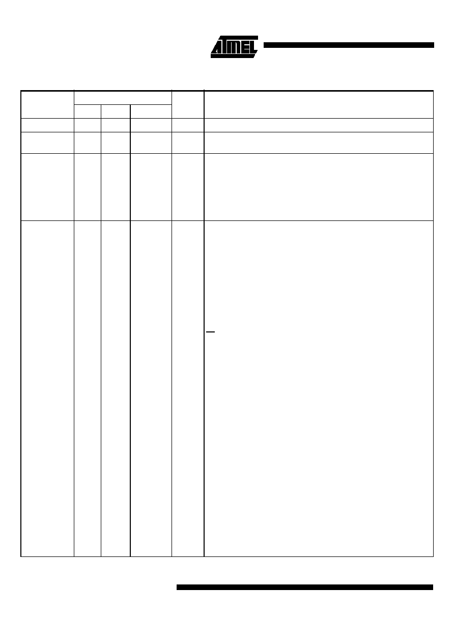
Table 12. Pin Description for 40 - 44 Pin Packages
Mnemonic
Pin Number
Type
Name and Function
DIL
LCC
VQFP44 1.4
VSS
20
22
16
I
Ground: 0V reference
VCC
40
44
38
I
Power Supply: This is the power supply voltage for normal, idle and power-down
operation
P0.0 - P0.7
39 - 32
43 - 36
37 - 30
I/O
Port 0: Port 0 is an open-drain, bi-directional I/O port. Port 0 pins that have 1s
written to them float and can be used as high impedance inputs. Port 0 must be
polarized to VCC or VSS in order to prevent any parasitic current consumption. Port 0
is also the multiplexed low-order address and data bus during access to external
program and data memory. In this application, it uses strong internal pull-up when
emitting 1s. Port 0 also inputs the code Bytes during Flash programming. External
pull-ups are required during program verification during which P0 outputs the code
Bytes.
P1.0 - P1.7
1 - 8
2 - 9
40 - 44
1 - 3
I/O
Port 1: Port 1 is an 8-bit bi-directional I/O port with internal pull-ups. Port 1 pins that
have 1s written to them are pulled high by the internal pull-ups and can be used as
inputs. As inputs, Port 1 pins that are externally pulled low will source current
because of the internal pull-ups. Port 1 also receives the low-order address Byte
during memory programming and verification.
Alternate functions for AT89C51RB2/RC2 Port 1 include:
1
2
40
I/O
P1.0: Input/Output
I/O
T2 (P1.0): Timer/Counter 2 external count input/Clockout
2
3
41
I/O
P1.1: Input/Output
I
T2EX: Timer/Counter 2 Reload/Capture/Direction Control
I
SS: SPI Slave Select
3
4
42
I/O
P1.2: Input/Output
I
ECI: External Clock for the PCA
4
5
43
I/O
P1.3: Input/Output
I/O
CEX0: Capture/Compare External I/O for PCA Module 0
5
6
44
I/O
P1.4: Input/Output
I/O
CEX1: Capture/Compare External I/O for PCA Module 1
6
7
1
I/O
P1.5: Input/Output
I/O
CEX2: Capture/Compare External I/O for PCA Module 2
I/O
MISO: SPI Master Input Slave Output line
When SPI is in master mode, MISO receives data from the slave peripheral. When
SPI is in slave mode, MISO outputs data to the master controller.
7
8
2
I/O
P1.6: Input/Output
I/O
CEX3: Capture/Compare External I/O for PCA Module 3
I/O
SCK: SPI Serial Clock
SCK outputs clock to the slave peripheral
8
9
3
I/O
P1.7: Input/Output:
相关PDF资料 |
PDF描述 |
|---|---|
| VI-J0F-IY-F4 | CONVERTER MOD DC/DC 72V 50W |
| VI-J0F-IY-F3 | CONVERTER MOD DC/DC 72V 50W |
| VJ2225A332KBLAT4X | CAP CER 3300PF 630V 10% NP0 2225 |
| VI-J0F-IY-F2 | CONVERTER MOD DC/DC 72V 50W |
| VJ2225A472JBEAT4X | CAP CER 4700PF 500V 5% NP0 2225 |
相关代理商/技术参数 |
参数描述 |
|---|---|
| AT89C51RC-24AC | 功能描述:8位微控制器 -MCU 32K FLASH 4.0 TO 5.5V - 24MHZ RoHS:否 制造商:Silicon Labs 核心:8051 处理器系列:C8051F39x 数据总线宽度:8 bit 最大时钟频率:50 MHz 程序存储器大小:16 KB 数据 RAM 大小:1 KB 片上 ADC:Yes 工作电源电压:1.8 V to 3.6 V 工作温度范围:- 40 C to + 105 C 封装 / 箱体:QFN-20 安装风格:SMD/SMT |
| AT89C51RC-24AI | 功能描述:8位微控制器 -MCU 32K FLASH 4.0 TO 5.5V - 24MHZ RoHS:否 制造商:Silicon Labs 核心:8051 处理器系列:C8051F39x 数据总线宽度:8 bit 最大时钟频率:50 MHz 程序存储器大小:16 KB 数据 RAM 大小:1 KB 片上 ADC:Yes 工作电源电压:1.8 V to 3.6 V 工作温度范围:- 40 C to + 105 C 封装 / 箱体:QFN-20 安装风格:SMD/SMT |
| AT89C51RC-24AU | 功能描述:8位微控制器 -MCU 32K FLASH 4.0 TO 5.5V RoHS:否 制造商:Silicon Labs 核心:8051 处理器系列:C8051F39x 数据总线宽度:8 bit 最大时钟频率:50 MHz 程序存储器大小:16 KB 数据 RAM 大小:1 KB 片上 ADC:Yes 工作电源电压:1.8 V to 3.6 V 工作温度范围:- 40 C to + 105 C 封装 / 箱体:QFN-20 安装风格:SMD/SMT |
| AT89C51RC-24JC | 功能描述:8位微控制器 -MCU 32K FLASH 4.0 TO 5.5V - 24MHZ RoHS:否 制造商:Silicon Labs 核心:8051 处理器系列:C8051F39x 数据总线宽度:8 bit 最大时钟频率:50 MHz 程序存储器大小:16 KB 数据 RAM 大小:1 KB 片上 ADC:Yes 工作电源电压:1.8 V to 3.6 V 工作温度范围:- 40 C to + 105 C 封装 / 箱体:QFN-20 安装风格:SMD/SMT |
| AT89C51RC-24JI | 功能描述:8位微控制器 -MCU 32K FLASH 4.0 TO 5.5V - 24MHZ RoHS:否 制造商:Silicon Labs 核心:8051 处理器系列:C8051F39x 数据总线宽度:8 bit 最大时钟频率:50 MHz 程序存储器大小:16 KB 数据 RAM 大小:1 KB 片上 ADC:Yes 工作电源电压:1.8 V to 3.6 V 工作温度范围:- 40 C to + 105 C 封装 / 箱体:QFN-20 安装风格:SMD/SMT |
发布紧急采购,3分钟左右您将得到回复。