- 您现在的位置:买卖IC网 > PDF目录12030 > AT89C51RC2-3CSUM (Atmel)IC 8051 MCU FLASH 32K 40DIP PDF资料下载
参数资料
| 型号: | AT89C51RC2-3CSUM |
| 厂商: | Atmel |
| 文件页数: | 89/127页 |
| 文件大小: | 0K |
| 描述: | IC 8051 MCU FLASH 32K 40DIP |
| 产品培训模块: | MCU Product Line Introduction |
| 标准包装: | 216 |
| 系列: | 89C |
| 核心处理器: | 8051 |
| 芯体尺寸: | 8-位 |
| 速度: | 60MHz |
| 连通性: | SPI,UART/USART |
| 外围设备: | POR,PWM,WDT |
| 输入/输出数: | 32 |
| 程序存储器容量: | 32KB(32K x 8) |
| 程序存储器类型: | 闪存 |
| RAM 容量: | 1.25K x 8 |
| 电压 - 电源 (Vcc/Vdd): | 2.7 V ~ 5.5 V |
| 振荡器型: | 外部 |
| 工作温度: | -40°C ~ 85°C |
| 封装/外壳: | 40-DIP(0.600",15.24mm) |
| 包装: | 管件 |
| 配用: | AT89OCD-01-ND - USB EMULATOR FOR AT8XC51 MCU AT89STK-11-ND - KIT STARTER FOR AT89C51RX2 |
第1页第2页第3页第4页第5页第6页第7页第8页第9页第10页第11页第12页第13页第14页第15页第16页第17页第18页第19页第20页第21页第22页第23页第24页第25页第26页第27页第28页第29页第30页第31页第32页第33页第34页第35页第36页第37页第38页第39页第40页第41页第42页第43页第44页第45页第46页第47页第48页第49页第50页第51页第52页第53页第54页第55页第56页第57页第58页第59页第60页第61页第62页第63页第64页第65页第66页第67页第68页第69页第70页第71页第72页第73页第74页第75页第76页第77页第78页第79页第80页第81页第82页第83页第84页第85页第86页第87页第88页当前第89页第90页第91页第92页第93页第94页第95页第96页第97页第98页第99页第100页第101页第102页第103页第104页第105页第106页第107页第108页第109页第110页第111页第112页第113页第114页第115页第116页第117页第118页第119页第120页第121页第122页第123页第124页第125页第126页第127页
64
AT89C51RB2/RC2
4180E–8051–10/06
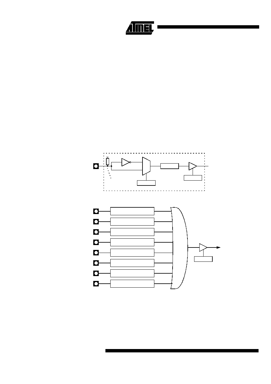
Keyboard Interface
The AT89C51RB2/RC2 implements a keyboard interface allowing the connection of a
8 x n matrix keyboard. It is based on 8 inputs with programmable interrupt capability on
both high or low level. These inputs are available as alternate function of P1 and allow to
exit from idle and power-down modes.
The keyboard interfaces with the C51 core through 3 special function registers: KBLS,
the Keyboard Level Selection register (Table 53), KBE, the Keyboard interrupt Enable
register (Table 52), and KBF, the Keyboard Flag register (Table 51).
Interrupt
The keyboard inputs are considered as 8 independent interrupt sources sharing the
same interrupt vector. An interrupt enable bit (KBD in IEN1) allows global enable or dis-
able of the keyboard interrupt (see Figure 23). As detailed in Figure 24 each keyboard
input has the capability to detect a programmable level according to KBLS. x bit value.
Level detection is then reported in interrupt flags KBF. x that can be masked by software
using KBE. x bits.
This structure allows keyboard arrangement from 1 by n to 8 by n matrix and allow
usage of P1 inputs for other purpose.
Figure 23. Keyboard Interface Block Diagram
Figure 24. Keyboard Input Circuitry
Power Reduction Mode
P1 inputs allow exit from idle and power down modes as detailed in Section “Power-
P1:x
KBE. x
KBF. x
KBLS. x
0
1
V
CC
Internal Pull-up
P1.0
Keyboard Interface
Interrupt Request
KBD
IEN1
Input Circuitry
P1.1
Input Circuitry
P1.2
Input Circuitry
P1.3
Input Circuitry
P1.4
Input Circuitry
P1.5
Input Circuitry
P1.6
Input Circuitry
P1.7
Input Circuitry
KBDIT
相关PDF资料 |
PDF描述 |
|---|---|
| VI-J0F-IY-F4 | CONVERTER MOD DC/DC 72V 50W |
| VI-J0F-IY-F3 | CONVERTER MOD DC/DC 72V 50W |
| VJ2225A332KBLAT4X | CAP CER 3300PF 630V 10% NP0 2225 |
| VI-J0F-IY-F2 | CONVERTER MOD DC/DC 72V 50W |
| VJ2225A472JBEAT4X | CAP CER 4700PF 500V 5% NP0 2225 |
相关代理商/技术参数 |
参数描述 |
|---|---|
| AT89C51RC-24AC | 功能描述:8位微控制器 -MCU 32K FLASH 4.0 TO 5.5V - 24MHZ RoHS:否 制造商:Silicon Labs 核心:8051 处理器系列:C8051F39x 数据总线宽度:8 bit 最大时钟频率:50 MHz 程序存储器大小:16 KB 数据 RAM 大小:1 KB 片上 ADC:Yes 工作电源电压:1.8 V to 3.6 V 工作温度范围:- 40 C to + 105 C 封装 / 箱体:QFN-20 安装风格:SMD/SMT |
| AT89C51RC-24AI | 功能描述:8位微控制器 -MCU 32K FLASH 4.0 TO 5.5V - 24MHZ RoHS:否 制造商:Silicon Labs 核心:8051 处理器系列:C8051F39x 数据总线宽度:8 bit 最大时钟频率:50 MHz 程序存储器大小:16 KB 数据 RAM 大小:1 KB 片上 ADC:Yes 工作电源电压:1.8 V to 3.6 V 工作温度范围:- 40 C to + 105 C 封装 / 箱体:QFN-20 安装风格:SMD/SMT |
| AT89C51RC-24AU | 功能描述:8位微控制器 -MCU 32K FLASH 4.0 TO 5.5V RoHS:否 制造商:Silicon Labs 核心:8051 处理器系列:C8051F39x 数据总线宽度:8 bit 最大时钟频率:50 MHz 程序存储器大小:16 KB 数据 RAM 大小:1 KB 片上 ADC:Yes 工作电源电压:1.8 V to 3.6 V 工作温度范围:- 40 C to + 105 C 封装 / 箱体:QFN-20 安装风格:SMD/SMT |
| AT89C51RC-24JC | 功能描述:8位微控制器 -MCU 32K FLASH 4.0 TO 5.5V - 24MHZ RoHS:否 制造商:Silicon Labs 核心:8051 处理器系列:C8051F39x 数据总线宽度:8 bit 最大时钟频率:50 MHz 程序存储器大小:16 KB 数据 RAM 大小:1 KB 片上 ADC:Yes 工作电源电压:1.8 V to 3.6 V 工作温度范围:- 40 C to + 105 C 封装 / 箱体:QFN-20 安装风格:SMD/SMT |
| AT89C51RC-24JI | 功能描述:8位微控制器 -MCU 32K FLASH 4.0 TO 5.5V - 24MHZ RoHS:否 制造商:Silicon Labs 核心:8051 处理器系列:C8051F39x 数据总线宽度:8 bit 最大时钟频率:50 MHz 程序存储器大小:16 KB 数据 RAM 大小:1 KB 片上 ADC:Yes 工作电源电压:1.8 V to 3.6 V 工作温度范围:- 40 C to + 105 C 封装 / 箱体:QFN-20 安装风格:SMD/SMT |
发布紧急采购,3分钟左右您将得到回复。