参数资料
| 型号: | AT89LS8252-12JI |
| 厂商: | Atmel |
| 文件页数: | 30/35页 |
| 文件大小: | 0K |
| 描述: | IC 8051 MCU FLASH 8K 44PLCC |
| 标准包装: | 27 |
| 系列: | 89LS |
| 核心处理器: | 8051 |
| 芯体尺寸: | 8-位 |
| 速度: | 12MHz |
| 连通性: | SPI,UART/USART |
| 外围设备: | POR,WDT |
| 输入/输出数: | 32 |
| 程序存储器容量: | 8KB(8K x 8) |
| 程序存储器类型: | 闪存 |
| EEPROM 大小: | 2K x 8 |
| RAM 容量: | 256 x 8 |
| 电压 - 电源 (Vcc/Vdd): | 2.7 V ~ 6 V |
| 振荡器型: | 内部 |
| 工作温度: | -40°C ~ 85°C |
| 封装/外壳: | 44-LCC(J 形引线) |
| 包装: | 管件 |
| 其它名称: | AT89LS825212JI |
第1页第2页第3页第4页第5页第6页第7页第8页第9页第10页第11页第12页第13页第14页第15页第16页第17页第18页第19页第20页第21页第22页第23页第24页第25页第26页第27页第28页第29页当前第30页第31页第32页第33页第34页第35页
AT89LS8252
0850C–MICRO–3/06
4
Pin Description
Furthermore, P1.4, P1.5, P1.6, and P1.7 can be configured
as the SPI slave port select, data input/output and shift
clock input/output pins as shown in the following table.
Port 1 also receives the low-order address bytes during
Flash programming and verification.
Port 2
Port 2 is an 8-bit bidirectional I/O port with internal pullups.
The Port 2 output buffers can sink/source four TTL inputs.
When 1s are written to Port 2 pins, they are pulled high by
the internal pullups and can be used as inputs. As inputs,
Port 2 pins that are externally being pulled low will source
current (IIL) because of the internal pullups.
Port 2 emits the high-order address byte during fetches
from external program memory and during accesses to
external data memory that use 16-bit addresses (MOVX @
DPTR). In this application, Port 2 uses strong internal pul-
lups when emitting 1s. During accesses to external data
memory that use 8-bit addresses (MOVX @ RI), Port 2
emits the contents of the P2 Special Function Register.
Port 2 also receives the high-order address bits and some
control signals during Flash programming and verification.
Port 3
Port 3 is an 8 bit bidirectional I/O port with internal pullups.
The Port 3 output buffers can sink/source four TTL inputs.
When 1s are written to Port 3 pins, they are pulled high by
the internal pullups and can be used as inputs. As inputs,
Port 3 pins that are externally being pulled low will source
current (IIL) because of the pullups.
Port 3 also serves the functions of various special features
of the AT89LS8252, as shown in the following table.
Port 3 also receives some control signals for Flash pro-
gramming and verification.
RST
Reset input. A high on this pin for two machine cycles while
the oscillator is running resets the device.
ALE/PROG
Address Latch Enable is an output pulse for latching the
low byte of the address during accesses to external mem-
ory. This pin is also the program pulse input (PROG) during
Flash programming.
In normal operation, ALE is emitted at a constant rate of 1/
6 the oscillator frequency and may be used for external tim-
ing or clocking purposes. Note, however, that one ALE
pulse is skipped during each access to external data mem-
ory.
If desired, ALE operation can be disabled by setting bit 0 of
SFR location 8EH. With the bit set, ALE is active only dur-
ing a MOVX or MOVC instruction. Otherwise, the pin is
weakly pulled high. Setting the ALE-disable bit has no
effect if the microcontroller is in external execution mode.
PSEN
Program Store Enable is the read strobe to external pro-
gram memory.
When the AT89LS8252 is executing code from external
program memory, PSEN is activated twice each machine
cycle, except that two PSEN activations are skipped during
each access to external data memory.
EA/VPP
External Access Enable. EA must be strapped to GND in
order to enable the device to fetch code from external pro-
gram memory locations starting at 0000H up to FFFFH.
Note, however, that if lock bit 1 is programmed, EA will be
internally latched on reset.
EA should be strapped to V
CC for internal program execu-
tions. This pin also receives the 12-volt programming
enable voltage (VPP) during Flash programming when 12-
volt programming is selected.
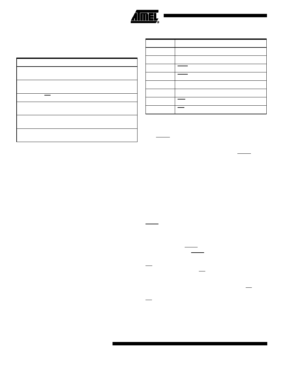
Port Pin
Alternate Functions
P1.0
T2 (external count input to Timer/Counter
2), clock-out
P1.1
T2EX (Timer/Counter 2 capture/reload
trigger and direction control)
P1.4
SS (Slave port select input)
P1.5
MOSI (Master data output, slave data input
pin for SPI channel)
P1.6
MISO (Master data input, slave data output
pin for SPI channel)
P1.7
SCK (Master clock output, slave clock input
pin for SPI channel)
Port Pin
Alternate Functions
P3.0
RXD (serial input port)
P3.1
TXD (serial output port)
P3.2
INT0 (external interrupt 0)
P3.3
INT1 (external interrupt 1)
P3.4
T0 (timer 0 external input)
P3.5
T1 (timer 1 external input)
P3.6
WR (external data memory write strobe)
P3.7
RD (external data memory read strobe)
相关PDF资料 |
PDF描述 |
|---|---|
| AT89LS8252-12JC | IC MICRO CTRL 12MHZ 44PLCC |
| AT89LS8252-12AI | IC 8051 MCU FLASH 8K 44TQFP |
| AT89LS8252-12AC | IC MICRO CTRL 12MHZ 44TQFP |
| AT89LS53-12PC | IC MICRO CTRL 12MHZ 40DIP |
| AT89LS53-12JI | IC 8051 MCU FLASH 12K 44PLCC |
相关代理商/技术参数 |
参数描述 |
|---|---|
| AT89LS8252-12PC | 功能描述:8位微控制器 -MCU Microcontroller RoHS:否 制造商:Silicon Labs 核心:8051 处理器系列:C8051F39x 数据总线宽度:8 bit 最大时钟频率:50 MHz 程序存储器大小:16 KB 数据 RAM 大小:1 KB 片上 ADC:Yes 工作电源电压:1.8 V to 3.6 V 工作温度范围:- 40 C to + 105 C 封装 / 箱体:QFN-20 安装风格:SMD/SMT |
| AT89LS8252-12PI | 功能描述:8位微控制器 -MCU Microcontroller RoHS:否 制造商:Silicon Labs 核心:8051 处理器系列:C8051F39x 数据总线宽度:8 bit 最大时钟频率:50 MHz 程序存储器大小:16 KB 数据 RAM 大小:1 KB 片上 ADC:Yes 工作电源电压:1.8 V to 3.6 V 工作温度范围:- 40 C to + 105 C 封装 / 箱体:QFN-20 安装风格:SMD/SMT |
| AT89LS8252-24QI | 功能描述:8位微控制器 -MCU Microcontroller RoHS:否 制造商:Silicon Labs 核心:8051 处理器系列:C8051F39x 数据总线宽度:8 bit 最大时钟频率:50 MHz 程序存储器大小:16 KB 数据 RAM 大小:1 KB 片上 ADC:Yes 工作电源电压:1.8 V to 3.6 V 工作温度范围:- 40 C to + 105 C 封装 / 箱体:QFN-20 安装风格:SMD/SMT |
| AT89LV51-12AC | 功能描述:8位微控制器 -MCU 80C31 w/4k RoHS:否 制造商:Silicon Labs 核心:8051 处理器系列:C8051F39x 数据总线宽度:8 bit 最大时钟频率:50 MHz 程序存储器大小:16 KB 数据 RAM 大小:1 KB 片上 ADC:Yes 工作电源电压:1.8 V to 3.6 V 工作温度范围:- 40 C to + 105 C 封装 / 箱体:QFN-20 安装风格:SMD/SMT |
| AT89LV51-12AI | 功能描述:8位微控制器 -MCU Microcontroller RoHS:否 制造商:Silicon Labs 核心:8051 处理器系列:C8051F39x 数据总线宽度:8 bit 最大时钟频率:50 MHz 程序存储器大小:16 KB 数据 RAM 大小:1 KB 片上 ADC:Yes 工作电源电压:1.8 V to 3.6 V 工作温度范围:- 40 C to + 105 C 封装 / 箱体:QFN-20 安装风格:SMD/SMT |
发布紧急采购,3分钟左右您将得到回复。