参数资料
| 型号: | AT89S51-24JU |
| 厂商: | Atmel |
| 文件页数: | 27/31页 |
| 文件大小: | 0K |
| 描述: | IC MCU 4K FLASH 24MHZ 44-PLCC |
| 产品培训模块: | MCU Product Line Introduction |
| 标准包装: | 27 |
| 系列: | 89S |
| 核心处理器: | 8051 |
| 芯体尺寸: | 8-位 |
| 速度: | 24MHz |
| 连通性: | UART/USART |
| 外围设备: | WDT |
| 输入/输出数: | 32 |
| 程序存储器容量: | 4KB(4K x 8) |
| 程序存储器类型: | 闪存 |
| RAM 容量: | 128 x 8 |
| 电压 - 电源 (Vcc/Vdd): | 4 V ~ 5.5 V |
| 振荡器型: | 内部 |
| 工作温度: | -40°C ~ 85°C |
| 封装/外壳: | 44-LCC(J 形引线) |
| 包装: | 管件 |
| 产品目录页面: | 616 (CN2011-ZH PDF) |
第1页第2页第3页第4页第5页第6页第7页第8页第9页第10页第11页第12页第13页第14页第15页第16页第17页第18页第19页第20页第21页第22页第23页第24页第25页第26页当前第27页第28页第29页第30页第31页
5
2487D–MICRO–6/08
AT89S51
nal pull-ups and can be used as inputs. As inputs, Port 3 pins that are externally being pulled low
will source current (I
IL) because of the pull-ups.
Port 3 receives some control signals for Flash programming and verification.
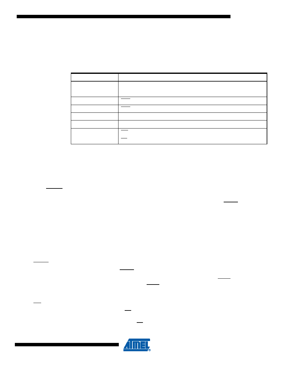
Port 3 also serves the functions of various special features of the AT89S51, as shown in the fol-
lowing table.
4.7
RST
Reset input. A high on this pin for two machine cycles while the oscillator is running resets
the device. This pin drives High for 98 oscillator periods after the Watchdog times out. The DIS-
RTO bit in SFR AUXR (address 8EH) can be used to disable this feature. In the default state of
bit DISRTO, the RESET HIGH out feature is enabled.
4.8
ALE/PROG
Address Latch Enable (ALE) is an output pulse for latching the low byte of the address during
accesses to external memory. This pin is also the program pulse input (PROG) during Flash
programming.
In normal operation, ALE is emitted at a constant rate of 1/6 the oscillator frequency and may be
used for external timing or clocking purposes. Note, however, that one ALE pulse is skipped dur-
ing each access to external data memory.
If desired, ALE operation can be disabled by setting bit 0 of SFR location 8EH. With the bit set,
ALE is active only during a MOVX or MOVC instruction. Otherwise, the pin is weakly pulled high.
Setting the ALE-disable bit has no effect if the microcontroller is in external execution mode.
4.9
PSEN
Program Store Enable (PSEN) is the read strobe to external program memory.
When the AT89S51 is executing code from external program memory, PSEN is activated twice
each machine cycle, except that two PSEN activations are skipped during each access to exter-
nal data memory.
4.10
EA/VPP
External Access Enable. EA must be strapped to GND in order to enable the device to fetch
code from external program memory locations starting at 0000H up to FFFFH. Note, however,
that if lock bit 1 is programmed, EA will be internally latched on reset.
Port Pin
Alternate Functions
P3.0
RXD (serial input port)
P3.1
TXD (serial output port)
P3.2
INT0 (external interrupt 0)
P3.3
INT1 (external interrupt 1)
P3.4
T0 (timer 0 external input)
P3.5
T1 (timer 1 external input)
P3.6
WR (external data memory write strobe)
P3.7
RD (external data memory read strobe)
相关PDF资料 |
PDF描述 |
|---|---|
| ATTINY2313A-MMH | IC MCU AVR 2K FLASH 20QFN |
| ATTINY84A-PU | MCU AVR 8K FLASH 20MHZ 14PDIP |
| ATTINY84A-CCU | IC MCU 8BIT 8K FLASH 15UFBGA |
| 008016038217751V | CABLE CLAMP W/STRAIN RELIEF #38 |
| 308237981000100 | COVER ASSMBLY FOR DIN CONN |
相关代理商/技术参数 |
参数描述 |
|---|---|
| AT89S51-24JU SL383 | 制造商:Atmel Corporation 功能描述:MCU 8-bit AT89 80C51 CISC 4KB Flash 5V 44-Pin PLCC T/R |
| AT89S51-24PC | 功能描述:8位微控制器 -MCU 4K ISP FLASH 2.7 TO 5.5V - 24 MHZ RoHS:否 制造商:Silicon Labs 核心:8051 处理器系列:C8051F39x 数据总线宽度:8 bit 最大时钟频率:50 MHz 程序存储器大小:16 KB 数据 RAM 大小:1 KB 片上 ADC:Yes 工作电源电压:1.8 V to 3.6 V 工作温度范围:- 40 C to + 105 C 封装 / 箱体:QFN-20 安装风格:SMD/SMT |
| AT89S51-24PI | 功能描述:8位微控制器 -MCU 4K ISP FLASH 2.7 TO 5.5V - 24 MHZ RoHS:否 制造商:Silicon Labs 核心:8051 处理器系列:C8051F39x 数据总线宽度:8 bit 最大时钟频率:50 MHz 程序存储器大小:16 KB 数据 RAM 大小:1 KB 片上 ADC:Yes 工作电源电压:1.8 V to 3.6 V 工作温度范围:- 40 C to + 105 C 封装 / 箱体:QFN-20 安装风格:SMD/SMT |
| AT89S51-24PU | 功能描述:8位微控制器 -MCU 4kB Flash 128B RAM 33MHz 4.0V-5.5V RoHS:否 制造商:Silicon Labs 核心:8051 处理器系列:C8051F39x 数据总线宽度:8 bit 最大时钟频率:50 MHz 程序存储器大小:16 KB 数据 RAM 大小:1 KB 片上 ADC:Yes 工作电源电压:1.8 V to 3.6 V 工作温度范围:- 40 C to + 105 C 封装 / 箱体:QFN-20 安装风格:SMD/SMT |
| AT89S51-24PU SL383 | 制造商:Atmel Corporation 功能描述:8051 4K ISP FLASH 4.0 TO 5.5V |
发布紧急采购,3分钟左右您将得到回复。