- 您现在的位置:买卖IC网 > PDF目录11794 > AT90CAN64-15AT1 (Atmel)MCU AVR 64K FLASH 15MHZ 64TQFP PDF资料下载
参数资料
| 型号: | AT90CAN64-15AT1 |
| 厂商: | Atmel |
| 文件页数: | 46/185页 |
| 文件大小: | 0K |
| 描述: | MCU AVR 64K FLASH 15MHZ 64TQFP |
| 产品培训模块: | MCU Product Line Introduction |
| 标准包装: | 1,000 |
| 系列: | AVR® 90CAN |
| 核心处理器: | AVR |
| 芯体尺寸: | 8-位 |
| 速度: | 16MHz |
| 连通性: | CAN,I²C,SPI,UART/USART |
| 外围设备: | 欠压检测/复位,POR,PWM,WDT |
| 输入/输出数: | 53 |
| 程序存储器容量: | 64KB(64K x 8) |
| 程序存储器类型: | 闪存 |
| EEPROM 大小: | 2K x 8 |
| RAM 容量: | 4K x 8 |
| 电压 - 电源 (Vcc/Vdd): | 2.7 V ~ 5.5 V |
| 数据转换器: | A/D 8x10b |
| 振荡器型: | 内部 |
| 工作温度: | -40°C ~ 105°C |
| 封装/外壳: | 64-TQFP |
| 包装: | 带卷 (TR) |
| 配用: | ATSTK600-ND - DEV KIT FOR AVR/AVR32 ATDVK90CAN1-ND - KIT DEV FOR AT90CAN128 MCU |
| 其它名称: | AT90CAN64-15AT1-ND AT90CAN64-15AT1TR |
第1页第2页第3页第4页第5页第6页第7页第8页第9页第10页第11页第12页第13页第14页第15页第16页第17页第18页第19页第20页第21页第22页第23页第24页第25页第26页第27页第28页第29页第30页第31页第32页第33页第34页第35页第36页第37页第38页第39页第40页第41页第42页第43页第44页第45页当前第46页第47页第48页第49页第50页第51页第52页第53页第54页第55页第56页第57页第58页第59页第60页第61页第62页第63页第64页第65页第66页第67页第68页第69页第70页第71页第72页第73页第74页第75页第76页第77页第78页第79页第80页第81页第82页第83页第84页第85页第86页第87页第88页第89页第90页第91页第92页第93页第94页第95页第96页第97页第98页第99页第100页第101页第102页第103页第104页第105页第106页第107页第108页第109页第110页第111页第112页第113页第114页第115页第116页第117页第118页第119页第120页第121页第122页第123页第124页第125页第126页第127页第128页第129页第130页第131页第132页第133页第134页第135页第136页第137页第138页第139页第140页第141页第142页第143页第144页第145页第146页第147页第148页第149页第150页第151页第152页第153页第154页第155页第156页第157页第158页第159页第160页第161页第162页第163页第164页第165页第166页第167页第168页第169页第170页第171页第172页第173页第174页第175页第176页第177页第178页第179页第180页第181页第182页第183页第184页第185页
14
7682C–AUTO–04/08
AT90CAN32/64/128
3.6
Stack Pointer
The Stack is mainly used for storing temporary data, for storing local variables and for storing
return addresses after interrupts and subroutine calls. The Stack Pointer Register always points
to the top of the Stack. Note that the Stack is implemented as growing from higher memory loca-
tions to lower memory locations. This implies that a Stack PUSH command decreases the Stack
Pointer.
The Stack Pointer points to the data SRAM Stack area where the Subroutine and Interrupt
Stacks are located. This Stack space in the data SRAM must be defined by the program before
any subroutine calls are executed or interrupts are enabled. The Stack Pointer must be set to
point above 0xFF. The Stack Pointer is decremented by one when data is pushed onto the Stack
with the PUSH instruction, and it is decremented by two when the return address is pushed onto
the Stack with subroutine call or interrupt. The Stack Pointer is incremented by one when data is
popped from the Stack with the POP instruction, and it is incremented by two when data is
popped from the Stack with return from subroutine RET or return from interrupt RETI.
The AVR Stack Pointer is implemented as two 8-bit registers in the I/O space. The number of
bits actually used is implementation dependent. Note that the data space in some implementa-
tions of the AVR architecture is so small that only SPL is needed. In this case, the SPH Register
will not be present.
3.7
Instruction Execution Timing
This section describes the general access timing concepts for instruction execution. The AVR
CPU is driven by the CPU clock clkCPU, directly generated from the selected clock source for the
chip. No internal clock division is used.
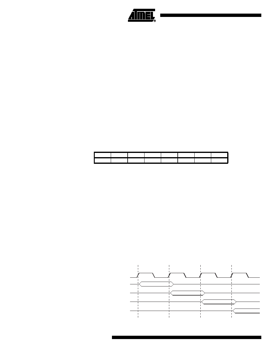
Figure 3-5 shows the parallel instruction fetches and instruction executions enabled by the Har-
vard architecture and the fast-access Register File concept. This is the basic pipelining concept
to obtain up to 1 MIPS per MHz with the corresponding unique results for functions per cost,
functions per clocks, and functions per power-unit.
Figure 3-5.
The Parallel Instruction Fetches and Instruction Executions
Bit
15
14
13
12
11
10
9
8
SP15
SP14
SP13
SP12
SP11
SP10
SP9
SP8
SPH
SP7
SP6
SP5
SP4
SP3
SP2
SP1
SP0
SPL
7
6
5
4
3
2
1
0
Read/Write
R/W
Initial Value
0
clk
1st Instruction Fetch
1st Instruction Execute
2nd Instruction Fetch
2nd Instruction Execute
3rd Instruction Fetch
3rd Instruction Execute
4th Instruction Fetch
T1
T2
T3
T4
CPU
相关PDF资料 |
PDF描述 |
|---|---|
| VI-B5W-IX-F2 | CONVERTER MOD DC/DC 5.5V 75W |
| VI-B5W-IX-F1 | CONVERTER MOD DC/DC 5.5V 75W |
| VI-B5V-IX-F4 | CONVERTER MOD DC/DC 5.8V 75W |
| VI-B5V-IX-F3 | CONVERTER MOD DC/DC 5.8V 75W |
| V48A36E500B | CONVERTER MOD DC/DC 36V 500W |
相关代理商/技术参数 |
参数描述 |
|---|---|
| AT90CAN64-15AZ | 功能描述:8位微控制器 -MCU 64KB Flash 15MHz RoHS:否 制造商:Silicon Labs 核心:8051 处理器系列:C8051F39x 数据总线宽度:8 bit 最大时钟频率:50 MHz 程序存储器大小:16 KB 数据 RAM 大小:1 KB 片上 ADC:Yes 工作电源电压:1.8 V to 3.6 V 工作温度范围:- 40 C to + 105 C 封装 / 箱体:QFN-20 安装风格:SMD/SMT |
| AT90CAN64-15MT | 功能描述:8位微控制器 -MCU 64KB Flash 15MHz RoHS:否 制造商:Silicon Labs 核心:8051 处理器系列:C8051F39x 数据总线宽度:8 bit 最大时钟频率:50 MHz 程序存储器大小:16 KB 数据 RAM 大小:1 KB 片上 ADC:Yes 工作电源电压:1.8 V to 3.6 V 工作温度范围:- 40 C to + 105 C 封装 / 箱体:QFN-20 安装风格:SMD/SMT |
| AT90CAN64-15MT1 | 功能描述:8位微控制器 -MCU 64KB Flash 15MHz RoHS:否 制造商:Silicon Labs 核心:8051 处理器系列:C8051F39x 数据总线宽度:8 bit 最大时钟频率:50 MHz 程序存储器大小:16 KB 数据 RAM 大小:1 KB 片上 ADC:Yes 工作电源电压:1.8 V to 3.6 V 工作温度范围:- 40 C to + 105 C 封装 / 箱体:QFN-20 安装风格:SMD/SMT |
| AT90CAN64-15MZ | 功能描述:8位微控制器 -MCU 64KB Flash 15MHz RoHS:否 制造商:Silicon Labs 核心:8051 处理器系列:C8051F39x 数据总线宽度:8 bit 最大时钟频率:50 MHz 程序存储器大小:16 KB 数据 RAM 大小:1 KB 片上 ADC:Yes 工作电源电压:1.8 V to 3.6 V 工作温度范围:- 40 C to + 105 C 封装 / 箱体:QFN-20 安装风格:SMD/SMT |
| AT90CAN64-16AI | 功能描述:8位微控制器 -MCU Microcontroller RoHS:否 制造商:Silicon Labs 核心:8051 处理器系列:C8051F39x 数据总线宽度:8 bit 最大时钟频率:50 MHz 程序存储器大小:16 KB 数据 RAM 大小:1 KB 片上 ADC:Yes 工作电源电压:1.8 V to 3.6 V 工作温度范围:- 40 C to + 105 C 封装 / 箱体:QFN-20 安装风格:SMD/SMT |
发布紧急采购,3分钟左右您将得到回复。