- 您现在的位置:买卖IC网 > PDF目录11216 > AT90PWM1-16MU (Atmel)IC AVR PWM 8KB FLASH 16MHZ 32QFN PDF资料下载
参数资料
| 型号: | AT90PWM1-16MU |
| 厂商: | Atmel |
| 文件页数: | 57/90页 |
| 文件大小: | 0K |
| 描述: | IC AVR PWM 8KB FLASH 16MHZ 32QFN |
| 产品培训模块: | megaAVR Introduction |
| 标准包装: | 1 |
| 系列: | AVR® 90PWM 照明 |
| 核心处理器: | AVR |
| 芯体尺寸: | 8-位 |
| 速度: | 16MHz |
| 连通性: | SPI |
| 外围设备: | 欠压检测/复位,POR,PWM,WDT |
| 输入/输出数: | 19 |
| 程序存储器容量: | 8KB(8K x 8) |
| 程序存储器类型: | 闪存 |
| EEPROM 大小: | 512 x 8 |
| RAM 容量: | 512 x 8 |
| 电压 - 电源 (Vcc/Vdd): | 2.7 V ~ 5.5 V |
| 数据转换器: | A/D 8x10b |
| 振荡器型: | 内部 |
| 工作温度: | -40°C ~ 105°C |
| 封装/外壳: | 32-VQFN 裸露焊盘 |
| 包装: | 标准包装 |
| 其它名称: | AT90PWM1-16MUDKR |
第1页第2页第3页第4页第5页第6页第7页第8页第9页第10页第11页第12页第13页第14页第15页第16页第17页第18页第19页第20页第21页第22页第23页第24页第25页第26页第27页第28页第29页第30页第31页第32页第33页第34页第35页第36页第37页第38页第39页第40页第41页第42页第43页第44页第45页第46页第47页第48页第49页第50页第51页第52页第53页第54页第55页第56页当前第57页第58页第59页第60页第61页第62页第63页第64页第65页第66页第67页第68页第69页第70页第71页第72页第73页第74页第75页第76页第77页第78页第79页第80页第81页第82页第83页第84页第85页第86页第87页第88页第89页第90页
60
4378C–AVR–09/08
AT90PWM1
If PORTxn is written logic one when the pin is configured as an output pin, the port pin is driven
high (one). If PORTxn is written logic zero when the pin is configured as an output pin, the port
pin is driven low (zero).
11.2.2
Toggling the Pin
Writing a logic one to PINxn toggles the value of PORTxn, independent on the value of DDRxn.
Note that the SBI instruction can be used to toggle one single bit in a port.
11.2.3
Switching Between Input and Output
When switching between tri-state ({DDxn, PORTxn} = 0b00) and output high ({DDxn, PORTxn}
= 0b11), an intermediate state with either pull-up enabled {DDxn, PORTxn} = 0b01) or output
low ({DDxn, PORTxn} = 0b10) must occur. Normally, the pull-up enabled state is fully accept-
able, as a high-impedant environment will not notice the difference between a strong high driver
and a pull-up. If this is not the case, the PUD bit in the MCUCR Register can be set to disable all
pull-ups in all ports.
Switching between input with pull-up and output low generates the same problem. The user
must use either the tri-state ({DDxn, PORTxn} = 0b00) or the output high state ({DDxn, PORTxn}
= 0b11) as an intermediate step.
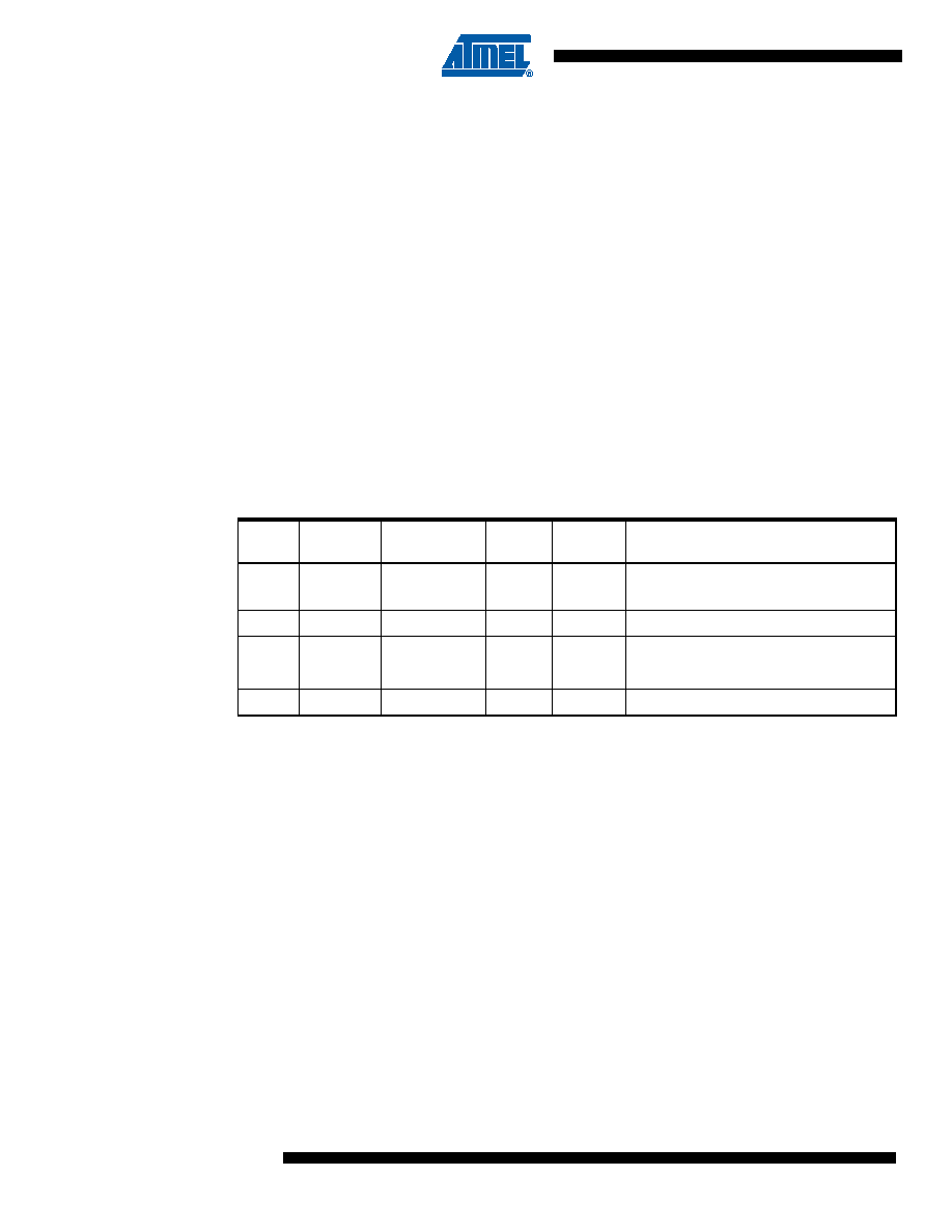
Table 7 summarizes the control signals for the pin value.
11.2.4
Reading the Pin Value
Independent of the setting of Data Direction bit DDxn, the port pin can be read through the
PINxn Register bit. As shown in Figure 11-2, the PINxn Register bit and the preceding latch con-
stitute a synchronizer. This is needed to avoid metastability if the physical pin changes value
near the edge of the internal clock, but it also introduces a delay. Figure 11-3 shows a timing dia-
gram of the synchronization when reading an externally applied pin value. The maximum and
minimum propagation delays are denoted tpd,max and tpd,min respectively.
Table 7. Port Pin Configurations
DDxn
PORTxn
PUD
(in MCUCR)
I/O
Pull-up
Comment
0
X
Input
No
Default configuration after Reset.
Tri-state (Hi-Z)
0
1
0
Input
Yes
Pxn will source current if ext. pulled low.
0
1
Input
No
Tri-state (Hi-Z)
1
0
X
Output
No
Output Low (Sink)
1
X
Output
No
Output High (Source)
相关PDF资料 |
PDF描述 |
|---|---|
| AT89C4051-24PU | IC MCU 4K FLASH 24MHZ 20-DIP |
| VE-B30-IX-F3 | CONVERTER MOD DC/DC 5V 75W |
| ADG731BCPZ-REEL | IC MULTIPLEXER 32X1 48LFCSP |
| ADG201HSKPZ-REEL | IC SWITCH QUAD SPST 20PLCC |
| ADG707BRU | IC MULTIPLEXER DUAL 8X1 28TSSOP |
相关代理商/技术参数 |
参数描述 |
|---|---|
| AT90PWM1-16MUR | 功能描述:8位微控制器 -MCU AVR 8KFLASH 2PSC, 16MHz RoHS:否 制造商:Silicon Labs 核心:8051 处理器系列:C8051F39x 数据总线宽度:8 bit 最大时钟频率:50 MHz 程序存储器大小:16 KB 数据 RAM 大小:1 KB 片上 ADC:Yes 工作电源电压:1.8 V to 3.6 V 工作温度范围:- 40 C to + 105 C 封装 / 箱体:QFN-20 安装风格:SMD/SMT |
| AT90PWM1-16SE | 制造商:Atmel Corporation 功能描述: |
| AT90PWM1-16SU | 功能描述:8位微控制器 -MCU AVR 8Kflash 2PSC No DALI 16MHz RoHS:否 制造商:Silicon Labs 核心:8051 处理器系列:C8051F39x 数据总线宽度:8 bit 最大时钟频率:50 MHz 程序存储器大小:16 KB 数据 RAM 大小:1 KB 片上 ADC:Yes 工作电源电压:1.8 V to 3.6 V 工作温度范围:- 40 C to + 105 C 封装 / 箱体:QFN-20 安装风格:SMD/SMT |
| AT90PWM161-16MN | 功能描述:8位微控制器 -MCU 16 MHz, QFN, 105oC, Green, RoHS:否 制造商:Silicon Labs 核心:8051 处理器系列:C8051F39x 数据总线宽度:8 bit 最大时钟频率:50 MHz 程序存储器大小:16 KB 数据 RAM 大小:1 KB 片上 ADC:Yes 工作电源电压:1.8 V to 3.6 V 工作温度范围:- 40 C to + 105 C 封装 / 箱体:QFN-20 安装风格:SMD/SMT |
| AT90PWM161-16MNR | 功能描述:8位微控制器 -MCU 16 MHz, QFN, 105oC, Green, T&R RoHS:否 制造商:Silicon Labs 核心:8051 处理器系列:C8051F39x 数据总线宽度:8 bit 最大时钟频率:50 MHz 程序存储器大小:16 KB 数据 RAM 大小:1 KB 片上 ADC:Yes 工作电源电压:1.8 V to 3.6 V 工作温度范围:- 40 C to + 105 C 封装 / 箱体:QFN-20 安装风格:SMD/SMT |
发布紧急采购,3分钟左右您将得到回复。