- 您现在的位置:买卖IC网 > PDF目录12058 > AT90PWM1-16SU (Atmel)MCU AVR 8K FLASH 16MHZ 24-SOIC PDF资料下载
参数资料
| 型号: | AT90PWM1-16SU |
| 厂商: | Atmel |
| 文件页数: | 58/90页 |
| 文件大小: | 0K |
| 描述: | MCU AVR 8K FLASH 16MHZ 24-SOIC |
| 产品培训模块: | MCU Product Line Introduction megaAVR Introduction |
| 标准包装: | 1,116 |
| 系列: | AVR® 90PWM 照明 |
| 核心处理器: | AVR |
| 芯体尺寸: | 8-位 |
| 速度: | 16MHz |
| 连通性: | SPI |
| 外围设备: | 欠压检测/复位,POR,PWM,WDT |
| 输入/输出数: | 19 |
| 程序存储器容量: | 8KB(8K x 8) |
| 程序存储器类型: | 闪存 |
| EEPROM 大小: | 512 x 8 |
| RAM 容量: | 512 x 8 |
| 电压 - 电源 (Vcc/Vdd): | 2.7 V ~ 5.5 V |
| 数据转换器: | A/D 8x10b |
| 振荡器型: | 内部 |
| 工作温度: | -40°C ~ 105°C |
| 封装/外壳: | 24-SOIC(0.295",7.50mm 宽) |
| 包装: | 管件 |
| 配用: | ATSTK600-RC19-ND - STK600 ROUTING CARD AVR ATSTK600-SOIC-ND - STK600 SOCKET/ADAPTER FOR SOIC |
第1页第2页第3页第4页第5页第6页第7页第8页第9页第10页第11页第12页第13页第14页第15页第16页第17页第18页第19页第20页第21页第22页第23页第24页第25页第26页第27页第28页第29页第30页第31页第32页第33页第34页第35页第36页第37页第38页第39页第40页第41页第42页第43页第44页第45页第46页第47页第48页第49页第50页第51页第52页第53页第54页第55页第56页第57页当前第58页第59页第60页第61页第62页第63页第64页第65页第66页第67页第68页第69页第70页第71页第72页第73页第74页第75页第76页第77页第78页第79页第80页第81页第82页第83页第84页第85页第86页第87页第88页第89页第90页
61
4378C–AVR–09/08
AT90PWM1
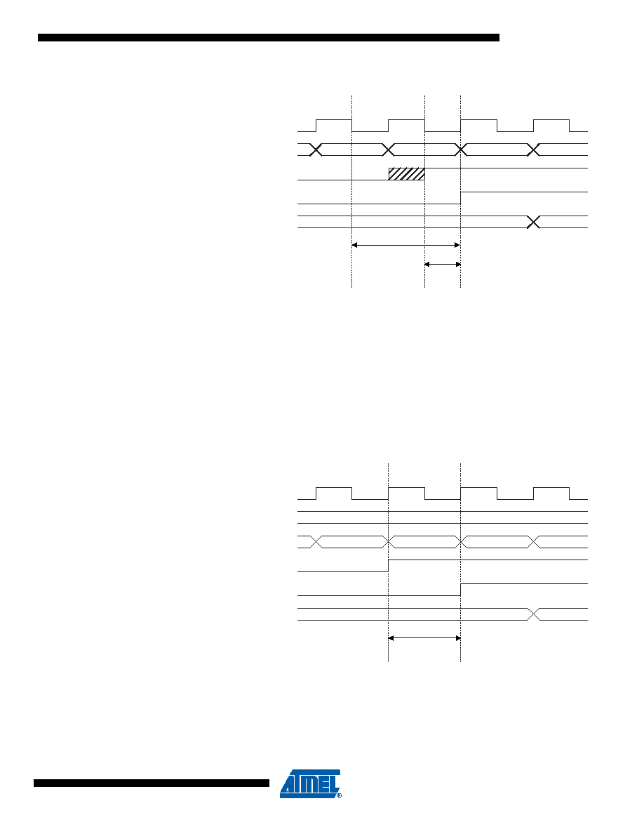
Figure 11-3.
Synchronization when Reading an Externally Applied Pin value
Consider the clock period starting shortly after the first falling edge of the system clock. The latch
is closed when the clock is low, and goes transparent when the clock is high, as indicated by the
shaded region of the “SYNC LATCH” signal. The signal value is latched when the system clock
goes low. It is clocked into the PINxn Register at the succeeding positive clock edge. As indi-
cated by the two arrows t
pd,max and tpd,min, a single signal transition on the pin will be delayed
between and 1 system clock period depending upon the time of assertion.
When reading back a software assigned pin value, a nop instruction must be inserted as indi-
cated in Figure 11-4. The out instruction sets the “SYNC LATCH” signal at the positive edge of
the clock. In this case, the delay t
pd through the synchronizer is 1 system clock period.
Figure 11-4.
Synchronization when Reading a Software Assigned Pin Value
The following code example shows how to set port B pins 0 and 1 high, 2 and 3 low, and define
the port pins from 4 to 7 as input with pull-ups assigned to port pins 6 and 7. The resulting pin
XXX
in r17, PINx
0x00
0xFF
INSTRUCTIONS
SYNC LATCH
PINxn
r17
XXX
SYSTEM CLK
t
pd, max
t pd, min
out PORTx, r16
nop
in r17, PINx
0xFF
0x00
0xFF
SYSTEM CLK
r16
INSTRUCTIONS
SYNC LATCH
PINxn
r17
t
pd
相关PDF资料 |
PDF描述 |
|---|---|
| VI-J0Y-IX-F1 | CONVERTER MOD DC/DC 3.3V 49.5W |
| AT89LP828-20AU | MCU 8051 8K FLASH SPI 32TQFP |
| VI-J0X-IY-F4 | CONVERTER MOD DC/DC 5.2V 50W |
| VI-JTL-IX-B1 | CONVERTER MOD DC/DC 28V 75W |
| AT89LP828-20MH | MCU 8051 8K FLASH SPI 32VQFN |
相关代理商/技术参数 |
参数描述 |
|---|---|
| AT90PWM161-16MN | 功能描述:8位微控制器 -MCU 16 MHz, QFN, 105oC, Green, RoHS:否 制造商:Silicon Labs 核心:8051 处理器系列:C8051F39x 数据总线宽度:8 bit 最大时钟频率:50 MHz 程序存储器大小:16 KB 数据 RAM 大小:1 KB 片上 ADC:Yes 工作电源电压:1.8 V to 3.6 V 工作温度范围:- 40 C to + 105 C 封装 / 箱体:QFN-20 安装风格:SMD/SMT |
| AT90PWM161-16MNR | 功能描述:8位微控制器 -MCU 16 MHz, QFN, 105oC, Green, T&R RoHS:否 制造商:Silicon Labs 核心:8051 处理器系列:C8051F39x 数据总线宽度:8 bit 最大时钟频率:50 MHz 程序存储器大小:16 KB 数据 RAM 大小:1 KB 片上 ADC:Yes 工作电源电压:1.8 V to 3.6 V 工作温度范围:- 40 C to + 105 C 封装 / 箱体:QFN-20 安装风格:SMD/SMT |
| AT90PWM161-16SN | 功能描述:8位微控制器 -MCU 16 MHz, SOIC, 105oC, Green RoHS:否 制造商:Silicon Labs 核心:8051 处理器系列:C8051F39x 数据总线宽度:8 bit 最大时钟频率:50 MHz 程序存储器大小:16 KB 数据 RAM 大小:1 KB 片上 ADC:Yes 工作电源电压:1.8 V to 3.6 V 工作温度范围:- 40 C to + 105 C 封装 / 箱体:QFN-20 安装风格:SMD/SMT |
| AT90PWM161-16SNR | 功能描述:8位微控制器 -MCU 16 MHz,SOIC,105oC, Green, T&R RoHS:否 制造商:Silicon Labs 核心:8051 处理器系列:C8051F39x 数据总线宽度:8 bit 最大时钟频率:50 MHz 程序存储器大小:16 KB 数据 RAM 大小:1 KB 片上 ADC:Yes 工作电源电压:1.8 V to 3.6 V 工作温度范围:- 40 C to + 105 C 封装 / 箱体:QFN-20 安装风格:SMD/SMT |
| AT90PWM161OS-16MNR | 功能描述:IC MCU 8BIT 16KB FLASH 32QFN 制造商:microchip technology 系列:AVR? 90PWM 照明 零件状态:在售 核心处理器:AVR 核心尺寸:8-位 速度:16MHz 连接性:SPI 外设:欠压检测/复位,POR,PWM,WDT I/O 数:20 程序存储容量:16KB(16K x 8) 程序存储器类型:闪存 EEPROM 容量:512 x 8 RAM 容量:1K x 8 电压 - 电源(Vcc/Vdd):2.7 V ~ 5.5 V 数据转换器:A/D 11x10b, D/A 1x10b 振荡器类型:内部 工作温度:-40°C ~ 105°C(TA) 标准包装:5,000 |
发布紧急采购,3分钟左右您将得到回复。