- 您现在的位置:买卖IC网 > PDF目录12035 > ATMEGA1284P-AU (Atmel)MCU AVR 128K ISP FLASH 44-TQFP PDF资料下载
参数资料
| 型号: | ATMEGA1284P-AU |
| 厂商: | Atmel |
| 文件页数: | 80/160页 |
| 文件大小: | 0K |
| 描述: | MCU AVR 128K ISP FLASH 44-TQFP |
| 产品培训模块: | MCU Product Line Introduction megaAVR Introduction |
| 标准包装: | 160 |
| 系列: | AVR® ATmega |
| 核心处理器: | AVR |
| 芯体尺寸: | 8-位 |
| 速度: | 20MHz |
| 连通性: | I²C,SPI,UART/USART |
| 外围设备: | 欠压检测/复位,POR,PWM,WDT |
| 输入/输出数: | 32 |
| 程序存储器容量: | 128KB(64K x 16) |
| 程序存储器类型: | 闪存 |
| EEPROM 大小: | 4K x 8 |
| RAM 容量: | 16K x 8 |
| 电压 - 电源 (Vcc/Vdd): | 1.8 V ~ 5.5 V |
| 数据转换器: | A/D 8x10b |
| 振荡器型: | 内部 |
| 工作温度: | -40°C ~ 85°C |
| 封装/外壳: | 44-TQFP |
| 包装: | 托盘 |
| 产品目录页面: | 614 (CN2011-ZH PDF) |
| 配用: | ATSTK600-RC31-ND - STK600 ROUTING CARD AVR ATSTK600-TQFP44-ND - STK600 SOCKET/ADAPTER 44-TQFP ATSTK600-ND - DEV KIT FOR AVR/AVR32 |
第1页第2页第3页第4页第5页第6页第7页第8页第9页第10页第11页第12页第13页第14页第15页第16页第17页第18页第19页第20页第21页第22页第23页第24页第25页第26页第27页第28页第29页第30页第31页第32页第33页第34页第35页第36页第37页第38页第39页第40页第41页第42页第43页第44页第45页第46页第47页第48页第49页第50页第51页第52页第53页第54页第55页第56页第57页第58页第59页第60页第61页第62页第63页第64页第65页第66页第67页第68页第69页第70页第71页第72页第73页第74页第75页第76页第77页第78页第79页当前第80页第81页第82页第83页第84页第85页第86页第87页第88页第89页第90页第91页第92页第93页第94页第95页第96页第97页第98页第99页第100页第101页第102页第103页第104页第105页第106页第107页第108页第109页第110页第111页第112页第113页第114页第115页第116页第117页第118页第119页第120页第121页第122页第123页第124页第125页第126页第127页第128页第129页第130页第131页第132页第133页第134页第135页第136页第137页第138页第139页第140页第141页第142页第143页第144页第145页第146页第147页第148页第149页第150页第151页第152页第153页第154页第155页第156页第157页第158页第159页第160页
26
8272E–AVR–04/2013
ATmega164A/PA/324A/PA/644A/PA/1284/P
When the write access time has elapsed, the EEPE bit is cleared by hardware. The user soft-
ware can poll this bit and wait for a zero before writing the next byte. When EEPE has been set,
the CPU is halted for two cycles before the next instruction is executed.
Bit 0 – EERE: EEPROM Read Enable
The EEPROM Read Enable Signal EERE is the read strobe to the EEPROM. When the correct
address is set up in the EEAR Register, the EERE bit must be written to a logic one to trigger the
EEPROM read. The EEPROM read access takes one instruction, and the requested data is
available immediately. When the EEPROM is read, the CPU is halted for four cycles before the
next instruction is executed.
The user should poll the EEPE bit before starting the read operation. If a write operation is in
progress, it is neither possible to read the EEPROM, nor to change the EEAR Register.
The calibrated Oscillator is used to time the EEPROM accesses. Table 8-2 on page 26 lists the
typical programming time for EEPROM access from the CPU.
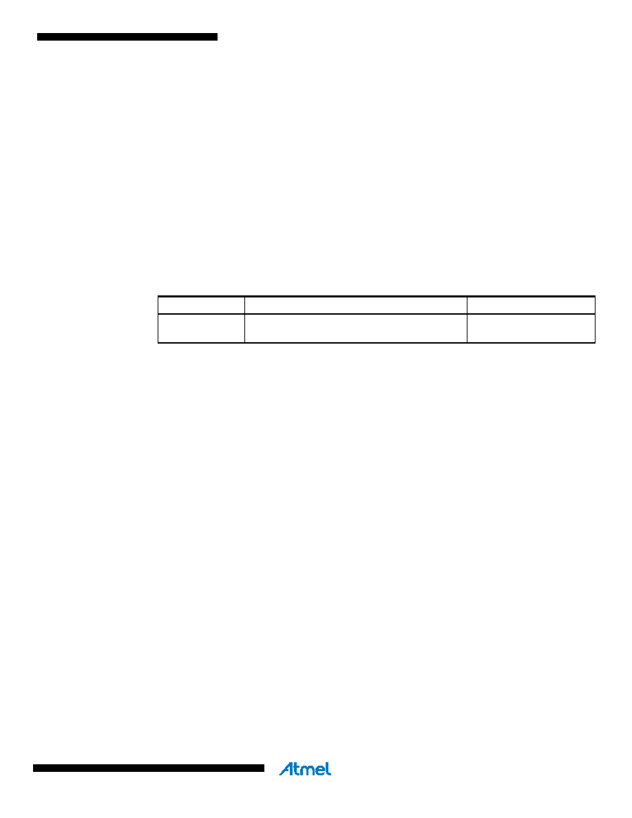
Table 8-2.
EEPROM programming time.
Symbol
Number of calibrated RC oscillator cycles
Typical programming time
EEPROM write
(from CPU)
26,368
3.3ms
相关PDF资料 |
PDF描述 |
|---|---|
| VE-JV1-IY-F4 | CONVERTER MOD DC/DC 12V 50W |
| ATMEGA1284P-MU | MCU AVR 128K ISP FLASH 44-QFN |
| VE-JV1-IY-F3 | CONVERTER MOD DC/DC 12V 50W |
| VE-B3Y-IX-F4 | CONVERTER MOD DC/DC 3.3V 49.5W |
| VE-B3Y-IX-F2 | CONVERTER MOD DC/DC 3.3V 49.5W |
相关代理商/技术参数 |
参数描述 |
|---|---|
| ATMEGA1284P-AUR | 功能描述:8位微控制器 -MCU AVR,128KB FLASH,1.8V 4KB EE 16KB SRAM RoHS:否 制造商:Silicon Labs 核心:8051 处理器系列:C8051F39x 数据总线宽度:8 bit 最大时钟频率:50 MHz 程序存储器大小:16 KB 数据 RAM 大小:1 KB 片上 ADC:Yes 工作电源电压:1.8 V to 3.6 V 工作温度范围:- 40 C to + 105 C 封装 / 箱体:QFN-20 安装风格:SMD/SMT |
| ATMEGA1284P-MU | 功能描述:8位微控制器 -MCU 128KB Flash 20MHz 1.8V-5.5V RoHS:否 制造商:Silicon Labs 核心:8051 处理器系列:C8051F39x 数据总线宽度:8 bit 最大时钟频率:50 MHz 程序存储器大小:16 KB 数据 RAM 大小:1 KB 片上 ADC:Yes 工作电源电压:1.8 V to 3.6 V 工作温度范围:- 40 C to + 105 C 封装 / 箱体:QFN-20 安装风格:SMD/SMT |
| ATMEGA1284P-MUR | 功能描述:8位微控制器 -MCU AVR,128KB FLASH,1.8V 4KB EE 16KB SRAM RoHS:否 制造商:Silicon Labs 核心:8051 处理器系列:C8051F39x 数据总线宽度:8 bit 最大时钟频率:50 MHz 程序存储器大小:16 KB 数据 RAM 大小:1 KB 片上 ADC:Yes 工作电源电压:1.8 V to 3.6 V 工作温度范围:- 40 C to + 105 C 封装 / 箱体:QFN-20 安装风格:SMD/SMT |
| ATMEGA1284P-PU | 功能描述:8位微控制器 -MCU 128KB Flash 20MHz 1.8V-5.5V RoHS:否 制造商:Silicon Labs 核心:8051 处理器系列:C8051F39x 数据总线宽度:8 bit 最大时钟频率:50 MHz 程序存储器大小:16 KB 数据 RAM 大小:1 KB 片上 ADC:Yes 工作电源电压:1.8 V to 3.6 V 工作温度范围:- 40 C to + 105 C 封装 / 箱体:QFN-20 安装风格:SMD/SMT |
| ATMEGA1284PR212-AU | 功能描述:8位微控制器 -MCU ATmega 1284P-AU AT86RF212-ZU RoHS:否 制造商:Silicon Labs 核心:8051 处理器系列:C8051F39x 数据总线宽度:8 bit 最大时钟频率:50 MHz 程序存储器大小:16 KB 数据 RAM 大小:1 KB 片上 ADC:Yes 工作电源电压:1.8 V to 3.6 V 工作温度范围:- 40 C to + 105 C 封装 / 箱体:QFN-20 安装风格:SMD/SMT |
发布紧急采购,3分钟左右您将得到回复。