- 您现在的位置:买卖IC网 > PDF目录12050 > ATMEGA164A-CU (Atmel)IC MCU AVR 16K 20MHZ 49VFBGA PDF资料下载
参数资料
| 型号: | ATMEGA164A-CU |
| 厂商: | Atmel |
| 文件页数: | 53/160页 |
| 文件大小: | 0K |
| 描述: | IC MCU AVR 16K 20MHZ 49VFBGA |
| 产品培训模块: | MCU Product Line Introduction megaAVR Introduction |
| 标准包装: | 490 |
| 系列: | AVR® ATmega |
| 核心处理器: | AVR |
| 芯体尺寸: | 8-位 |
| 速度: | 20MHz |
| 连通性: | I²C,SPI,UART/USART |
| 外围设备: | 欠压检测/复位,POR,PWM,WDT |
| 输入/输出数: | 32 |
| 程序存储器容量: | 16KB(8K x 16) |
| 程序存储器类型: | 闪存 |
| EEPROM 大小: | 512 x 8 |
| RAM 容量: | 1K x 8 |
| 电压 - 电源 (Vcc/Vdd): | 1.8 V ~ 5.5 V |
| 数据转换器: | A/D 8x10b |
| 振荡器型: | 内部 |
| 工作温度: | -40°C ~ 85°C |
| 封装/外壳: | 49-VFBGA |
| 包装: | 托盘 |
第1页第2页第3页第4页第5页第6页第7页第8页第9页第10页第11页第12页第13页第14页第15页第16页第17页第18页第19页第20页第21页第22页第23页第24页第25页第26页第27页第28页第29页第30页第31页第32页第33页第34页第35页第36页第37页第38页第39页第40页第41页第42页第43页第44页第45页第46页第47页第48页第49页第50页第51页第52页当前第53页第54页第55页第56页第57页第58页第59页第60页第61页第62页第63页第64页第65页第66页第67页第68页第69页第70页第71页第72页第73页第74页第75页第76页第77页第78页第79页第80页第81页第82页第83页第84页第85页第86页第87页第88页第89页第90页第91页第92页第93页第94页第95页第96页第97页第98页第99页第100页第101页第102页第103页第104页第105页第106页第107页第108页第109页第110页第111页第112页第113页第114页第115页第116页第117页第118页第119页第120页第121页第122页第123页第124页第125页第126页第127页第128页第129页第130页第131页第132页第133页第134页第135页第136页第137页第138页第139页第140页第141页第142页第143页第144页第145页第146页第147页第148页第149页第150页第151页第152页第153页第154页第155页第156页第157页第158页第159页第160页
146
8272E–AVR–04/2013
ATmega164A/PA/324A/PA/644A/PA/1284/P
according to operating mode set by the WGM22:0 bits and Compare Output mode (COM2x1:0)
bits. The max and bottom signals are used by the Waveform Generator for handling the special
cases of the extreme values in some modes of operation (see ”Modes of operation” on page
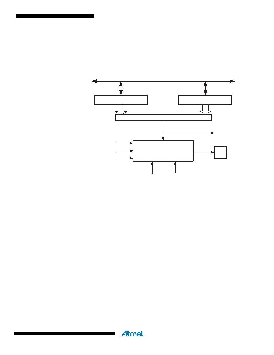
Figure 16-10 on page 131 shows a block diagram of the Output Compare unit.
Figure 17-3. Output Compare unit, block diagram.
The OCR2x Register is double buffered when using any of the Pulse Width Modulation (PWM)
modes. For the Normal and Clear Timer on Compare (CTC) modes of operation, the double
buffering is disabled. The double buffering synchronizes the update of the OCR2x Compare
Register to either top or bottom of the counting sequence. The synchronization prevents the
occurrence of odd-length, non-symmetrical PWM pulses, thereby making the output glitch-free.
The OCR2x Register access may seem complex, but this is not case. When the double buffering
is enabled, the CPU has access to the OCR2x Buffer Register, and if double buffering is dis-
abled the CPU will access the OCR2x directly.
17.5.1
Force Output Compare
In non-PWM waveform generation modes, the match output of the comparator can be forced by
writing a one to the Force Output Compare (FOC2x) bit. Forcing compare match will not set the
OCF2x Flag or reload/clear the timer, but the OC2x pin will be updated as if a real compare
match had occurred (the COM2x1:0 bits settings define whether the OC2x pin is set, cleared or
toggled).
17.5.2
Compare Match Blocking by TCNT2 Write
All CPU write operations to the TCNT2 Register will block any compare match that occurs in the
next timer clock cycle, even when the timer is stopped. This feature allows OCR2x to be initial-
ized to the same value as TCNT2 without triggering an interrupt when the Timer/Counter clock is
enabled.
OCFnx (Int.Req.)
= (8-bit Comparator )
OCRnx
OCnx
DATA BUS
TCNTn
WGMn1:0
Waveform Generator
top
FOCn
COMnX1:0
bottom
相关PDF资料 |
PDF描述 |
|---|---|
| VE-J0T-IY-F2 | CONVERTER MOD DC/DC 6.5V 50W |
| VE-JW2-IX-B1 | CONVERTER MOD DC/DC 15V 75W |
| VE-JW1-IX-B1 | CONVERTER MOD DC/DC 12V 75W |
| VJ1825A102KBCAT4X | CAP CER 1000PF 200V 10% NP0 1825 |
| VE-J1W-IX-B1 | CONVERTER MOD DC/DC 5.5V 75W |
相关代理商/技术参数 |
参数描述 |
|---|---|
| ATMEGA164A-CUR | 功能描述:8位微控制器 -MCU AVR 16KB FL 512B EE 1KB SRAM-20 MHz RoHS:否 制造商:Silicon Labs 核心:8051 处理器系列:C8051F39x 数据总线宽度:8 bit 最大时钟频率:50 MHz 程序存储器大小:16 KB 数据 RAM 大小:1 KB 片上 ADC:Yes 工作电源电压:1.8 V to 3.6 V 工作温度范围:- 40 C to + 105 C 封装 / 箱体:QFN-20 安装风格:SMD/SMT |
| ATMEGA164A-MCH | 功能描述:8位微控制器 -MCU AVR 16KB FL 512B EE 1KB SRAM-20 MHz RoHS:否 制造商:Silicon Labs 核心:8051 处理器系列:C8051F39x 数据总线宽度:8 bit 最大时钟频率:50 MHz 程序存储器大小:16 KB 数据 RAM 大小:1 KB 片上 ADC:Yes 工作电源电压:1.8 V to 3.6 V 工作温度范围:- 40 C to + 105 C 封装 / 箱体:QFN-20 安装风格:SMD/SMT |
| ATMEGA164A-MCHR | 功能描述:8位微控制器 -MCU AVR 16KB FL 512B EE 1KB SRAM-20 MHz RoHS:否 制造商:Silicon Labs 核心:8051 处理器系列:C8051F39x 数据总线宽度:8 bit 最大时钟频率:50 MHz 程序存储器大小:16 KB 数据 RAM 大小:1 KB 片上 ADC:Yes 工作电源电压:1.8 V to 3.6 V 工作温度范围:- 40 C to + 105 C 封装 / 箱体:QFN-20 安装风格:SMD/SMT |
| ATMEGA164A-MU | 功能描述:8位微控制器 -MCU AVR 16KB FL 512B EE 1KB SRAM-20 MHz RoHS:否 制造商:Silicon Labs 核心:8051 处理器系列:C8051F39x 数据总线宽度:8 bit 最大时钟频率:50 MHz 程序存储器大小:16 KB 数据 RAM 大小:1 KB 片上 ADC:Yes 工作电源电压:1.8 V to 3.6 V 工作温度范围:- 40 C to + 105 C 封装 / 箱体:QFN-20 安装风格:SMD/SMT |
| ATMEGA164A-MUR | 功能描述:8位微控制器 -MCU AVR 16KB FL 512B EE 1KB SRAM-20 MHz RoHS:否 制造商:Silicon Labs 核心:8051 处理器系列:C8051F39x 数据总线宽度:8 bit 最大时钟频率:50 MHz 程序存储器大小:16 KB 数据 RAM 大小:1 KB 片上 ADC:Yes 工作电源电压:1.8 V to 3.6 V 工作温度范围:- 40 C to + 105 C 封装 / 箱体:QFN-20 安装风格:SMD/SMT |
发布紧急采购,3分钟左右您将得到回复。