- 您现在的位置:买卖IC网 > PDF目录12052 > ATMEGA16A-PU (Atmel)MCU AVR 16K FLASH 16MHZ 40-PDIP PDF资料下载
参数资料
| 型号: | ATMEGA16A-PU |
| 厂商: | Atmel |
| 文件页数: | 31/88页 |
| 文件大小: | 0K |
| 描述: | MCU AVR 16K FLASH 16MHZ 40-PDIP |
| 产品培训模块: | MCU Product Line Introduction megaAVR Introduction |
| 标准包装: | 10 |
| 系列: | AVR® ATmega |
| 核心处理器: | AVR |
| 芯体尺寸: | 8-位 |
| 速度: | 16MHz |
| 连通性: | I²C,SPI,UART/USART |
| 外围设备: | 欠压检测/复位,POR,PWM,WDT |
| 输入/输出数: | 32 |
| 程序存储器容量: | 16KB(8K x 16) |
| 程序存储器类型: | 闪存 |
| EEPROM 大小: | 512 x 8 |
| RAM 容量: | 1K x 8 |
| 电压 - 电源 (Vcc/Vdd): | 2.7 V ~ 5.5 V |
| 数据转换器: | A/D 8x10b |
| 振荡器型: | 内部 |
| 工作温度: | -40°C ~ 85°C |
| 封装/外壳: | 40-DIP(0.600",15.24mm) |
| 包装: | 管件 |
| 配用: | ATSTK600-RC05-ND - STK600 ROUTING CARD AVR ATSTK600-ND - DEV KIT FOR AVR/AVR32 ATSTK500-ND - PROGRAMMER AVR STARTER KIT |
第1页第2页第3页第4页第5页第6页第7页第8页第9页第10页第11页第12页第13页第14页第15页第16页第17页第18页第19页第20页第21页第22页第23页第24页第25页第26页第27页第28页第29页第30页当前第31页第32页第33页第34页第35页第36页第37页第38页第39页第40页第41页第42页第43页第44页第45页第46页第47页第48页第49页第50页第51页第52页第53页第54页第55页第56页第57页第58页第59页第60页第61页第62页第63页第64页第65页第66页第67页第68页第69页第70页第71页第72页第73页第74页第75页第76页第77页第78页第79页第80页第81页第82页第83页第84页第85页第86页第87页第88页
2009 Microchip Technology Inc.
DS41288F-page 129
PIC16F610/616/16HV610/616
13.0
INSTRUCTION SET SUMMARY
The PIC16F610/616/16HV610/616 instruction set is
highly orthogonal and is comprised of three basic
categories:
Byte-oriented operations
Bit-oriented operations
Literal and control operations
Each PIC16 instruction is a 14-bit word divided into an
opcode, which specifies the instruction type and one or
more operands, which further specify the operation of
the instruction. The formats for each of the categories
is presented in Figure 13-1, while the various opcode
fields are summarized in Table 13-1.
Table 13-2 lists the instructions recognized by the
MPASMTM assembler.
For byte-oriented instructions, ‘f’ represents a file
register designator and ‘d’ represents a destination
designator. The file register designator specifies which
file register is to be used by the instruction.
The destination designator specifies where the result of
the operation is to be placed. If ‘d’ is zero, the result is
placed in the W register. If ‘d’ is one, the result is placed
in the file register specified in the instruction.
For bit-oriented instructions, ‘b’ represents a bit field
designator, which selects the bit affected by the
operation, while ‘f’ represents the address of the file in
which the bit is located.
For literal and control operations, ‘k’ represents an
8-bit or 11-bit constant, or literal value.
One instruction cycle consists of four oscillator periods;
for an oscillator frequency of 4 MHz, this gives a normal
instruction execution time of 1
μs. All instructions are
executed within a single instruction cycle, unless a
conditional test is true, or the program counter is
changed as a result of an instruction. When this occurs,
the execution takes two instruction cycles, with the
second cycle executed as a NOP.
All instruction examples use the format ‘0xhh’ to
represent a hexadecimal number, where ‘h’ signifies a
hexadecimal digit.
13.1
Read-Modify-Write Operations
Any instruction that specifies a file register as part of
the instruction performs a Read-Modify-Write (RMW)
operation. The register is read, the data is modified,
and the result is stored according to either the instruc-
tion or the destination designator ‘d’. A read operation
is performed on a register even if the instruction writes
to that register.
For example, a CLRF
PORTA
instruction will read
PORTA, clear all the data bits, then write the result
back to PORTA. This example would have the unin-
tended consequence of clearing the condition that set
the RAIF flag.
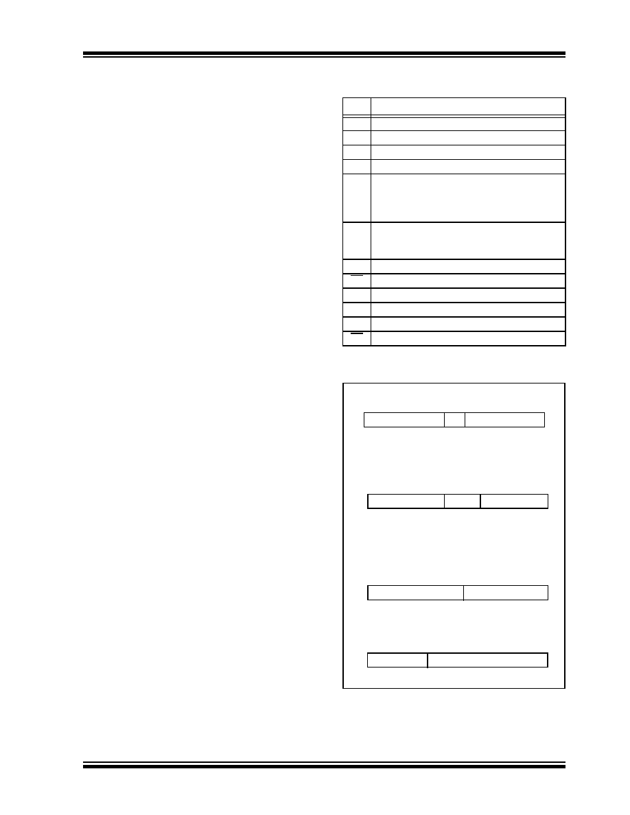
TABLE 13-1:
OPCODE FIELD
DESCRIPTIONS
FIGURE 13-1:
GENERAL FORMAT FOR
INSTRUCTIONS
Field
Description
f
Register file address (0x00 to 0x7F)
W
Working register (accumulator)
b
Bit address within an 8-bit file register
k
Literal field, constant data or label
x
Don’t care location (= 0 or 1).
The assembler will generate code with x = 0.
It is the recommended form of use for
compatibility with all Microchip software tools.
d
Destination select; d = 0: store result in W,
d = 1: store result in file register f.
Default is d = 1.
PC
Program Counter
TO
Time-out bit
C
Carry bit
DC
Digit carry bit
Z
Zero bit
PD
Power-down bit
Byte-oriented file register operations
13
8
7
6
0
d = 0 for destination W
OPCODE
d
f (FILE #)
d = 1 for destination f
f = 7-bit file register address
Bit-oriented file register operations
13
10 9
7 6
0
OPCODE
b (BIT #)
f (FILE #)
b = 3-bit address
f = 7-bit file register address
Literal and control operations
13
8
7
0
OPCODE
k (literal)
k = 8-bit immediate value
13
11
10
0
OPCODE
k (literal)
k = 11-bit immediate value
General
CALL
and GOTO instructions only
相关PDF资料 |
PDF描述 |
|---|---|
| VI-J04-IX-B1 | CONVERTER MOD DC/DC 48V 75W |
| VI-J03-IX-B1 | CONVERTER MOD DC/DC 24V 75W |
| VI-JTY-IY-F4 | CONVERTER MOD DC/DC 3.3V 33W |
| VI-JTY-IY-F2 | CONVERTER MOD DC/DC 3.3V 33W |
| ATMEGA164A-MU | IC MCU AVR 16K 20MHZ 44VQFN |
相关代理商/技术参数 |
参数描述 |
|---|---|
| ATMEGA16HVA | 制造商:ATMEL 制造商全称:ATMEL Corporation 功能描述:8-bit Microcontroller with 8K/16K Bytes In-System Programmable Flash |
| ATMEGA16HVA-4CKU | 功能描述:8位微控制器 -MCU 16KB Flash Memory 1.8V - 9.0V Supply RoHS:否 制造商:Silicon Labs 核心:8051 处理器系列:C8051F39x 数据总线宽度:8 bit 最大时钟频率:50 MHz 程序存储器大小:16 KB 数据 RAM 大小:1 KB 片上 ADC:Yes 工作电源电压:1.8 V to 3.6 V 工作温度范围:- 40 C to + 105 C 封装 / 箱体:QFN-20 安装风格:SMD/SMT |
| ATMEGA16HVA-4CKUR | 功能描述:8位微控制器 -MCU AVR batman 16KB FLSH 4 MHZ,LGA,GRN1.8-9V RoHS:否 制造商:Silicon Labs 核心:8051 处理器系列:C8051F39x 数据总线宽度:8 bit 最大时钟频率:50 MHz 程序存储器大小:16 KB 数据 RAM 大小:1 KB 片上 ADC:Yes 工作电源电压:1.8 V to 3.6 V 工作温度范围:- 40 C to + 105 C 封装 / 箱体:QFN-20 安装风格:SMD/SMT |
| ATMEGA16HVA-4TU | 功能描述:8位微控制器 -MCU 16KB Flash Memory 1.8V - 9.0V Supply RoHS:否 制造商:Silicon Labs 核心:8051 处理器系列:C8051F39x 数据总线宽度:8 bit 最大时钟频率:50 MHz 程序存储器大小:16 KB 数据 RAM 大小:1 KB 片上 ADC:Yes 工作电源电压:1.8 V to 3.6 V 工作温度范围:- 40 C to + 105 C 封装 / 箱体:QFN-20 安装风格:SMD/SMT |
| ATMEGA16HVA-4TUR | 功能描述:8位微控制器 -MCU AVR batman 16KB FLSH 4 MHZ TSOP, 1.8-9V RoHS:否 制造商:Silicon Labs 核心:8051 处理器系列:C8051F39x 数据总线宽度:8 bit 最大时钟频率:50 MHz 程序存储器大小:16 KB 数据 RAM 大小:1 KB 片上 ADC:Yes 工作电源电压:1.8 V to 3.6 V 工作温度范围:- 40 C to + 105 C 封装 / 箱体:QFN-20 安装风格:SMD/SMT |
发布紧急采购,3分钟左右您将得到回复。