参数资料
| 型号: | ATMEGA324PA-CU |
| 厂商: | Atmel |
| 文件页数: | 65/160页 |
| 文件大小: | 0K |
| 描述: | MCU AVR 32K FLASH 20MHZ BGA |
| 产品培训模块: | MCU Product Line Introduction megaAVR Introduction |
| 标准包装: | 525 |
| 系列: | AVR® ATmega |
| 核心处理器: | AVR |
| 芯体尺寸: | 8-位 |
| 速度: | 20MHz |
| 连通性: | I²C,SPI,UART/USART |
| 外围设备: | 欠压检测/复位,POR,PWM,WDT |
| 输入/输出数: | 32 |
| 程序存储器容量: | 32KB(16K x 16) |
| 程序存储器类型: | 闪存 |
| EEPROM 大小: | 1K x 8 |
| RAM 容量: | 2K x 8 |
| 电压 - 电源 (Vcc/Vdd): | 1.8 V ~ 5.5 V |
| 数据转换器: | A/D 8x10b |
| 振荡器型: | 内部 |
| 工作温度: | -40°C ~ 85°C |
| 封装/外壳: | 49-VFBGA |
| 包装: | 托盘 |
| 配用: | ATSTK600-ND - DEV KIT FOR AVR/AVR32 |
第1页第2页第3页第4页第5页第6页第7页第8页第9页第10页第11页第12页第13页第14页第15页第16页第17页第18页第19页第20页第21页第22页第23页第24页第25页第26页第27页第28页第29页第30页第31页第32页第33页第34页第35页第36页第37页第38页第39页第40页第41页第42页第43页第44页第45页第46页第47页第48页第49页第50页第51页第52页第53页第54页第55页第56页第57页第58页第59页第60页第61页第62页第63页第64页当前第65页第66页第67页第68页第69页第70页第71页第72页第73页第74页第75页第76页第77页第78页第79页第80页第81页第82页第83页第84页第85页第86页第87页第88页第89页第90页第91页第92页第93页第94页第95页第96页第97页第98页第99页第100页第101页第102页第103页第104页第105页第106页第107页第108页第109页第110页第111页第112页第113页第114页第115页第116页第117页第118页第119页第120页第121页第122页第123页第124页第125页第126页第127页第128页第129页第130页第131页第132页第133页第134页第135页第136页第137页第138页第139页第140页第141页第142页第143页第144页第145页第146页第147页第148页第149页第150页第151页第152页第153页第154页第155页第156页第157页第158页第159页第160页
157
8272E–AVR–04/2013
ATmega164A/PA/324A/PA/644A/PA/1284/P
17.11 Register description
17.11.1
TCCR2A – Timer/Counter Control Register A
Bits 7:6 – COM2A1:0: Compare Match Output A Mode
These bits control the Output Compare pin (OC2A) behavior. If one or both of the COM2A1:0
bits are set, the OC2A output overrides the normal port functionality of the I/O pin it is connected
to. However, note that the Data Direction Register (DDR) bit corresponding to the OC2A pin
must be set in order to enable the output driver.
When OC2A is connected to the pin, the function of the COM2A1:0 bits depends on the
WGM22:0 bit setting. Table 17-2 shows the COM2A1:0 bit functionality when the WGM22:0 bits
are set to a normal or CTC mode (non-PWM).
Table 17-3 shows the COM2A1:0 bit functionality when the WGM21:0 bits are set to fast PWM
mode.
Note:
1. A special case occurs when OCR2A equals TOP and COM2A1 is set. In this case, the Com-
pare Match is ignored, but the set or clear is done at BOTTOM. See ”Fast PWM mode” on
page 149 for more details.
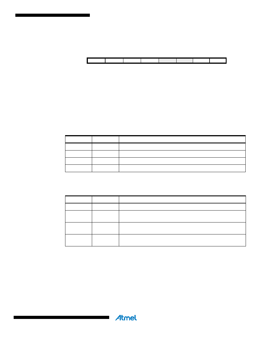
Bit
7
6
5
4
3
210
COM2A1
COM2A0
COM2B1
COM2B0
–
WGM21
WGM20
TCCR2A
Read/Write
R/W
R
R/W
Initial Value
0
Table 17-2.
Compare Output mode, non-PWM mode.
COM2A1
COM2A0
Description
0
Normal port operation, OC0A disconnected.
0
1
Toggle OC2A on Compare Match
1
0
Clear OC2A on Compare Match
1
Set OC2A on Compare Match
Table 17-3.
Compare Output mode, fast PWM mode
(1).
COM2A1
COM2A0
Description
0
Normal port operation, OC2A disconnected.
01
WGM22 = 0: Normal Port Operation, OC0A Disconnected.
WGM22 = 1: Toggle OC2A on Compare Match.
10
Clear OC2A on Compare Match, set OC2A at BOTTOM,
(non-inverting mode).
11
Set OC2A on Compare Match, clear OC2A at BOTTOM,
(inverting mode).
相关PDF资料 |
PDF描述 |
|---|---|
| ATSAM3N4BA-MU | MCU FLASH 64-QFN |
| ATSAM3N1AA-MU | MCU FLASH 48-QFN |
| ATUC64D4-Z1UT | IC MCU 32BIT 64KB FLASH 48QFN |
| ATUC64D4-AUT | IC MCU 32BIT 64KB FLASH 48TQFP |
| AT91SAM7S32B-AU | IC MCU ARM7 32KB FLASH 48LQFP |
相关代理商/技术参数 |
参数描述 |
|---|---|
| ATMEGA324PA-CUR | 功能描述:8位微控制器 -MCU AVR 32KB FLSH 1KB EE 2KB SRAM-20MHz IND RoHS:否 制造商:Silicon Labs 核心:8051 处理器系列:C8051F39x 数据总线宽度:8 bit 最大时钟频率:50 MHz 程序存储器大小:16 KB 数据 RAM 大小:1 KB 片上 ADC:Yes 工作电源电压:1.8 V to 3.6 V 工作温度范围:- 40 C to + 105 C 封装 / 箱体:QFN-20 安装风格:SMD/SMT |
| ATMEGA324PA-D | 功能描述:8位微控制器 -MCU AVR 32KB 1KB EE 20MHz 2KB SRAM 5V RoHS:否 制造商:Silicon Labs 核心:8051 处理器系列:C8051F39x 数据总线宽度:8 bit 最大时钟频率:50 MHz 程序存储器大小:16 KB 数据 RAM 大小:1 KB 片上 ADC:Yes 工作电源电压:1.8 V to 3.6 V 工作温度范围:- 40 C to + 105 C 封装 / 箱体:QFN-20 安装风格:SMD/SMT |
| ATMEGA324PA-MCH | 功能描述:8位微控制器 -MCU AVR 32KB 1KB EE 20MHz 2KB SRAM 5V RoHS:否 制造商:Silicon Labs 核心:8051 处理器系列:C8051F39x 数据总线宽度:8 bit 最大时钟频率:50 MHz 程序存储器大小:16 KB 数据 RAM 大小:1 KB 片上 ADC:Yes 工作电源电压:1.8 V to 3.6 V 工作温度范围:- 40 C to + 105 C 封装 / 箱体:QFN-20 安装风格:SMD/SMT |
| ATMEGA324PA-MCHR | 功能描述:8位微控制器 -MCU AVR 32KB FLSH 1KB EE 2KB SRAM-20MHz IND RoHS:否 制造商:Silicon Labs 核心:8051 处理器系列:C8051F39x 数据总线宽度:8 bit 最大时钟频率:50 MHz 程序存储器大小:16 KB 数据 RAM 大小:1 KB 片上 ADC:Yes 工作电源电压:1.8 V to 3.6 V 工作温度范围:- 40 C to + 105 C 封装 / 箱体:QFN-20 安装风格:SMD/SMT |
| ATMEGA324PA-MN | 功能描述:8位微控制器 -MCU AVR 32KB FLSH 1KB EE 2KB SRAM-20MHz 105C RoHS:否 制造商:Silicon Labs 核心:8051 处理器系列:C8051F39x 数据总线宽度:8 bit 最大时钟频率:50 MHz 程序存储器大小:16 KB 数据 RAM 大小:1 KB 片上 ADC:Yes 工作电源电压:1.8 V to 3.6 V 工作温度范围:- 40 C to + 105 C 封装 / 箱体:QFN-20 安装风格:SMD/SMT |
发布紧急采购,3分钟左右您将得到回复。