参数资料
| 型号: | ATMEGA328P-15AZ |
| 厂商: | Atmel |
| 文件页数: | 48/83页 |
| 文件大小: | 0K |
| 描述: | MCU AVR 32K FLASH 15MHZ 32-TQFP |
| 产品培训模块: | megaAVR Introduction |
| 标准包装: | 1 |
| 系列: | AVR® ATmega |
| 核心处理器: | AVR |
| 芯体尺寸: | 8-位 |
| 速度: | 16MHz |
| 连通性: | I²C,SPI,UART/USART |
| 外围设备: | 欠压检测/复位,POR,PWM,WDT |
| 输入/输出数: | 23 |
| 程序存储器容量: | 32KB(16K x 16) |
| 程序存储器类型: | 闪存 |
| EEPROM 大小: | 1K x 8 |
| RAM 容量: | 2K x 8 |
| 电压 - 电源 (Vcc/Vdd): | 2.7 V ~ 5.5 V |
| 数据转换器: | A/D 8x10b |
| 振荡器型: | 内部 |
| 工作温度: | -40°C ~ 125°C |
| 封装/外壳: | 32-TQFP |
| 包装: | 剪切带 (CT) |
| 其它名称: | ATMEGA328P-15AZCT |
第1页第2页第3页第4页第5页第6页第7页第8页第9页第10页第11页第12页第13页第14页第15页第16页第17页第18页第19页第20页第21页第22页第23页第24页第25页第26页第27页第28页第29页第30页第31页第32页第33页第34页第35页第36页第37页第38页第39页第40页第41页第42页第43页第44页第45页第46页第47页当前第48页第49页第50页第51页第52页第53页第54页第55页第56页第57页第58页第59页第60页第61页第62页第63页第64页第65页第66页第67页第68页第69页第70页第71页第72页第73页第74页第75页第76页第77页第78页第79页第80页第81页第82页第83页
PIC12(L)F1822/PIC16(L)F1823
DS41413C-page 210
2010-2012 Microchip Technology Inc.
24.3
PWM Overview
Pulse-Width Modulation (PWM) is a scheme that
provides power to a load by switching quickly between
fully on and fully off states. The PWM signal resembles
a square wave where the high portion of the signal is
considered the on state and the low portion of the signal
is considered the off state. The high portion, also known
as the pulse width, can vary in time and is defined in
steps. A larger number of steps applied, which
lengthens the pulse width, also supplies more power to
the load. Lowering the number of steps applied, which
shortens the pulse width, supplies less power. The
PWM period is defined as the duration of one complete
cycle or the total amount of on and off time combined.
PWM resolution defines the maximum number of steps
that can be present in a single PWM period. A higher
resolution allows for more precise control of the pulse
width time and in turn the power that is applied to the
load.
The term duty cycle describes the proportion of the on
time to the off time and is expressed in percentages,
where 0% is fully off and 100% is fully on. A lower duty
cycle corresponds to less power applied and a higher
duty cycle corresponds to more power applied.
Figure 24-3 shows a typical waveform of the PWM
signal.
24.3.1
STANDARD PWM OPERATION
The standard PWM mode generates a Pulse-Width
modulation (PWM) signal on the CCP1 pin with up to 10
bits of resolution. The period, duty cycle, and resolution
are controlled by the following registers:
PR2 registers
T2CON registers
CCPR1L registers
CCP1CON registers
Figure 24-4 shows a simplified block diagram of PWM
operation.
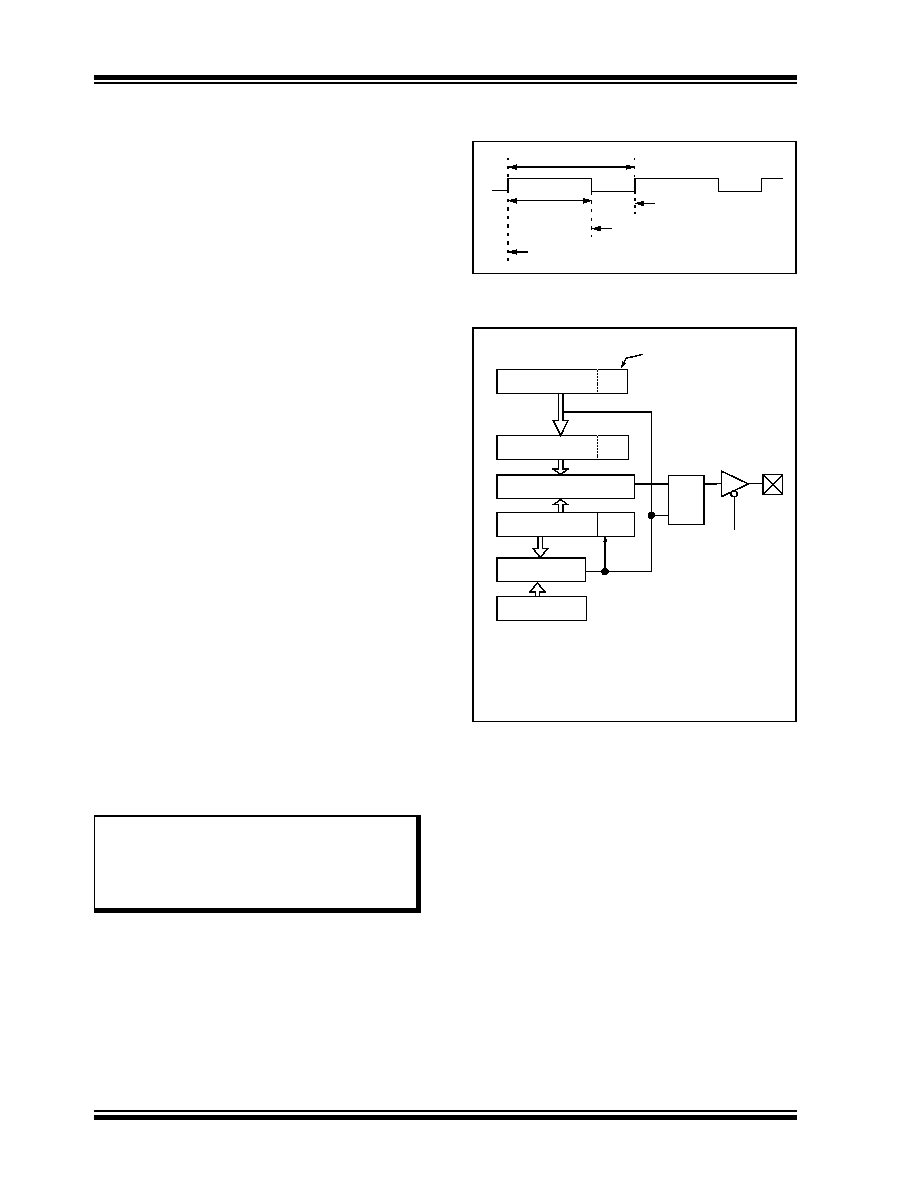
FIGURE 24-3:
CCP1 PWM OUTPUT
SIGNAL
FIGURE 24-4:
SIMPLIFIED PWM BLOCK
DIAGRAM
Note 1:
The corresponding TRIS bit must be
cleared to enable the PWM output on the
CCP1 pin.
2:
Clearing the CCP1CON register will
relinquish control of the CCP1 pin.
Period
Pulse Width
TMR2 = 0
TMR2 = CCPR1H:CCP1CON<5:4>
TMR2 = PR2
CCPR1L
CCPR1H(2) (Slave)
Comparator
TMR2
PR2
(1)
RQ
S
Duty Cycle Registers
CCP1CON<5:4>
Clear Timer,
toggle CCP1 pin and
latch duty cycle
Note
1:
The 8-bit timer TMR2 register is concatenated
with the 2-bit internal system clock (FOSC), or
two bits of the prescaler, to create the 10-bit
time base.
2:
In PWM mode, CCPR1H is a read-only register.
TRIS
CCP1
Comparator
相关PDF资料 |
PDF描述 |
|---|---|
| ATMEGA32L-8PJ | IC MCU AVR 32K 5V 8MHZ 40-DIP |
| ATMEGA32M1-AUR | IC MPU AVR 32K 20MHZ 32TQFP |
| ATMEGA48PA-MMNR | MCU AVR 4KB FLASH 20MHZ 28QFN |
| ATMEGA644P-B15MZ | IC MCU 8BIT 64KB FLASH 32VQFN |
| ATMEGA644V-10PU | IC AVR MCU FLASH 64K 40DIP |
相关代理商/技术参数 |
参数描述 |
|---|---|
| ATMEGA328P-15MZ | 功能描述:8位微控制器 -MCU 32KB In-system Flash 20MHz 1.8V-5.5V RoHS:否 制造商:Silicon Labs 核心:8051 处理器系列:C8051F39x 数据总线宽度:8 bit 最大时钟频率:50 MHz 程序存储器大小:16 KB 数据 RAM 大小:1 KB 片上 ADC:Yes 工作电源电压:1.8 V to 3.6 V 工作温度范围:- 40 C to + 105 C 封装 / 箱体:QFN-20 安装风格:SMD/SMT |
| ATMEGA328P-20AU | 制造商:Atmel Corporation 功能描述:MCU 8-bit ATmega AVR RISC 32KB Flash 3.3V/5V 32-Pin TQFP |
| ATMEGA328P20MU | 制造商:Atmel Corporation 功能描述:MCU 8-Bit ATmega AVR RISC 32KB Flash 3.3V/5V 32-Pin MLF |
| ATMEGA328P-AN | 功能描述:8位微控制器 -MCU AVR 32K FLSH 2K SRAM 1KB EE-20 MHZ 105C RoHS:否 制造商:Silicon Labs 核心:8051 处理器系列:C8051F39x 数据总线宽度:8 bit 最大时钟频率:50 MHz 程序存储器大小:16 KB 数据 RAM 大小:1 KB 片上 ADC:Yes 工作电源电压:1.8 V to 3.6 V 工作温度范围:- 40 C to + 105 C 封装 / 箱体:QFN-20 安装风格:SMD/SMT |
| ATMEGA328P-ANR | 功能描述:8位微控制器 -MCU AVR 32K FLSH 2K SRAM 1KB EE-20 MHZ 105C RoHS:否 制造商:Silicon Labs 核心:8051 处理器系列:C8051F39x 数据总线宽度:8 bit 最大时钟频率:50 MHz 程序存储器大小:16 KB 数据 RAM 大小:1 KB 片上 ADC:Yes 工作电源电压:1.8 V to 3.6 V 工作温度范围:- 40 C to + 105 C 封装 / 箱体:QFN-20 安装风格:SMD/SMT |
发布紧急采购,3分钟左右您将得到回复。