参数资料
| 型号: | ATTINY13A-SU |
| 厂商: | Atmel |
| 文件页数: | 13/67页 |
| 文件大小: | 0K |
| 描述: | IC MCU AVR 1K FLASH 20MHZ 8SOIC |
| 产品培训模块: | MCU Product Line Introduction tinyAVR Introduction |
| 标准包装: | 95 |
| 系列: | AVR® ATtiny |
| 核心处理器: | AVR |
| 芯体尺寸: | 8-位 |
| 速度: | 20MHz |
| 外围设备: | 欠压检测/复位,POR,PWM,WDT |
| 输入/输出数: | 6 |
| 程序存储器容量: | 1KB(512 x 16) |
| 程序存储器类型: | 闪存 |
| EEPROM 大小: | 64 x 8 |
| RAM 容量: | 64 x 8 |
| 电压 - 电源 (Vcc/Vdd): | 1.8 V ~ 5.5 V |
| 数据转换器: | A/D 4x10b |
| 振荡器型: | 内部 |
| 工作温度: | -40°C ~ 85°C |
| 封装/外壳: | 8-SOIC(0.209",5.30mm 宽) |
| 包装: | 管件 |
| 产品目录页面: | 612 (CN2011-ZH PDF) |
| 配用: | ATSTK600-DIP40-ND - STK600 SOCKET/ADAPTER 40-PDIP ATAVRDRAGON-ND - KIT DRAGON FLASH MEM AVR ATAVRISP2-ND - PROGRAMMER AVR IN SYSTEM ATJTAGICE2-ND - AVR ON-CHIP D-BUG SYSTEM |
第1页第2页第3页第4页第5页第6页第7页第8页第9页第10页第11页第12页当前第13页第14页第15页第16页第17页第18页第19页第20页第21页第22页第23页第24页第25页第26页第27页第28页第29页第30页第31页第32页第33页第34页第35页第36页第37页第38页第39页第40页第41页第42页第43页第44页第45页第46页第47页第48页第49页第50页第51页第52页第53页第54页第55页第56页第57页第58页第59页第60页第61页第62页第63页第64页第65页第66页第67页
12
8126F–AVR–05/12
ATtiny13A
4.6
Instruction Execution Timing
This section describes the general access timing concepts for instruction execution. The AVR
CPU is driven by the CPU clock clk
CPU, directly generated from the selected clock source for the
chip. No internal clock division is used.
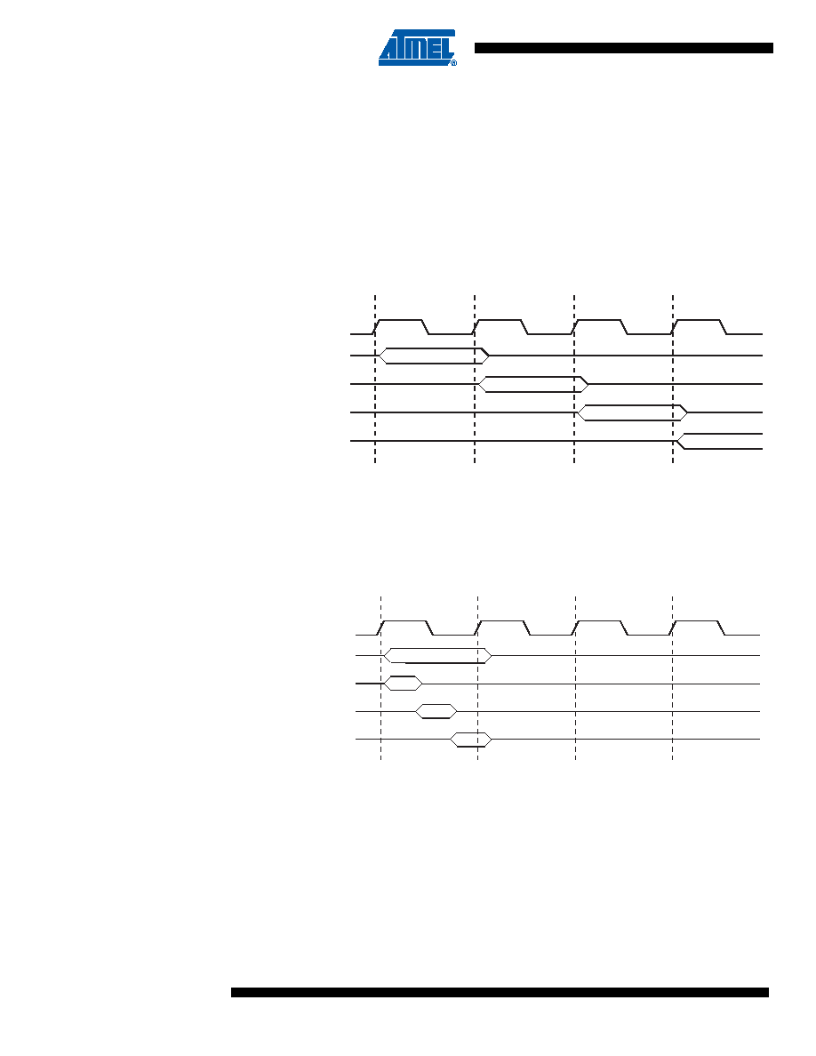
Figure 4-4 on page 12 shows the parallel instruction fetches and instruction executions enabled
by the Harvard architecture and the fast access Register File concept. This is the basic pipelin-
ing concept to obtain up to 1 MIPS per MHz with the corresponding unique results for functions
per cost, functions per clocks, and functions per power-unit.
Figure 4-4.
The Parallel Instruction Fetches and Instruction Executions
Figure 4-5 on page 12 shows the internal timing concept for the Register File. In a single clock
cycle an ALU operation using two register operands is executed, and the result is stored back to
the destination register.
Figure 4-5.
Single Cycle ALU Operation
4.7
Reset and Interrupt Handling
The AVR provides several different interrupt sources. These interrupts and the separate Reset
Vector each have a separate Program Vector in the Program memory space. All interrupts are
assigned individual enable bits which must be written logic one together with the Global Interrupt
Enable bit in the Status Register in order to enable the interrupt.
The lowest addresses in the Program memory space are by default defined as the Reset and
Interrupt Vectors. The complete list of vectors is shown in “Interrupts” on page 45. The list also
determines the priority levels of the different interrupts. The lower the address the higher is the
clk
1st Instruction Fetch
1st Instruction Execute
2nd Instruction Fetch
2nd Instruction Execute
3rd Instruction Fetch
3rd Instruction Execute
4th Instruction Fetch
T1
T2
T3
T4
CPU
Total Execution Time
Register Operands Fetch
ALU Operation Execute
Result Write Back
T1
T2
T3
T4
clk
CPU
相关PDF资料 |
PDF描述 |
|---|---|
| ATTINY13A-PU | IC MCU AVR 1K FLASH 20MHZ 8PDIP |
| ATTINY48-MUR | MCU AVR 4KB FLASH 12MHZ 32QFN |
| ATTINY13A-MU | IC MCU AVR 1K FLASH 20MHZ 20-QFN |
| ATTINY13A-SN | IC MCU AVR 1KB FLASH 20MHZ 8SOIC |
| ATTINY13A-SH | IC MCU AVR 1K FLASH 20MHZ 8SOIC |
相关代理商/技术参数 |
参数描述 |
|---|---|
| ATTINY13A-SU/LFCTC3136-01038 | 制造商:Atmel Corporation 功能描述:MCU 8BIT ATTINY RISC 1KB FLASH 2.5V/3.3V/5V 8SOIC EIAJ - Rail/Tube |
| ATTINY13A-SUR | 功能描述:8位微控制器 -MCU AVR 1KB FL 64B EE 64B SRAM 20 MHz IND RoHS:否 制造商:Silicon Labs 核心:8051 处理器系列:C8051F39x 数据总线宽度:8 bit 最大时钟频率:50 MHz 程序存储器大小:16 KB 数据 RAM 大小:1 KB 片上 ADC:Yes 工作电源电压:1.8 V to 3.6 V 工作温度范围:- 40 C to + 105 C 封装 / 箱体:QFN-20 安装风格:SMD/SMT |
| ATTINY13A-W | 功能描述:8位微控制器 -MCU Microcontroller RoHS:否 制造商:Silicon Labs 核心:8051 处理器系列:C8051F39x 数据总线宽度:8 bit 最大时钟频率:50 MHz 程序存储器大小:16 KB 数据 RAM 大小:1 KB 片上 ADC:Yes 工作电源电压:1.8 V to 3.6 V 工作温度范围:- 40 C to + 105 C 封装 / 箱体:QFN-20 安装风格:SMD/SMT |
| ATTINY13A-W-11 | 功能描述:8位微控制器 -MCU Microcontroller RoHS:否 制造商:Silicon Labs 核心:8051 处理器系列:C8051F39x 数据总线宽度:8 bit 最大时钟频率:50 MHz 程序存储器大小:16 KB 数据 RAM 大小:1 KB 片上 ADC:Yes 工作电源电压:1.8 V to 3.6 V 工作温度范围:- 40 C to + 105 C 封装 / 箱体:QFN-20 安装风格:SMD/SMT |
| ATTINY13-D | 功能描述:8位微控制器 -MCU Microcontroller RoHS:否 制造商:Silicon Labs 核心:8051 处理器系列:C8051F39x 数据总线宽度:8 bit 最大时钟频率:50 MHz 程序存储器大小:16 KB 数据 RAM 大小:1 KB 片上 ADC:Yes 工作电源电压:1.8 V to 3.6 V 工作温度范围:- 40 C to + 105 C 封装 / 箱体:QFN-20 安装风格:SMD/SMT |
发布紧急采购,3分钟左右您将得到回复。