参数资料
| 型号: | ATTINY13V-10SUR |
| 厂商: | Atmel |
| 文件页数: | 123/176页 |
| 文件大小: | 0K |
| 描述: | MCU AVR 1KB FLASH 10MHZ 8SOIC |
| 产品培训模块: | tinyAVR Introduction |
| 标准包装: | 2,000 |
| 系列: | AVR® ATtiny |
| 核心处理器: | AVR |
| 芯体尺寸: | 8-位 |
| 速度: | 10MHz |
| 外围设备: | 欠压检测/复位,POR,PWM,WDT |
| 输入/输出数: | 6 |
| 程序存储器容量: | 1KB(512 x 16) |
| 程序存储器类型: | 闪存 |
| EEPROM 大小: | 64 x 8 |
| RAM 容量: | 64 x 8 |
| 电压 - 电源 (Vcc/Vdd): | 1.8 V ~ 5.5 V |
| 数据转换器: | A/D 4x10b |
| 振荡器型: | 内部 |
| 工作温度: | -40°C ~ 85°C |
| 封装/外壳: | 8-SOIC(0.209",5.30mm 宽) |
| 包装: | 带卷 (TR) |
| 其它名称: | ATTINY13V-10SUR-ND ATTINY13V-10SURTR |
第1页第2页第3页第4页第5页第6页第7页第8页第9页第10页第11页第12页第13页第14页第15页第16页第17页第18页第19页第20页第21页第22页第23页第24页第25页第26页第27页第28页第29页第30页第31页第32页第33页第34页第35页第36页第37页第38页第39页第40页第41页第42页第43页第44页第45页第46页第47页第48页第49页第50页第51页第52页第53页第54页第55页第56页第57页第58页第59页第60页第61页第62页第63页第64页第65页第66页第67页第68页第69页第70页第71页第72页第73页第74页第75页第76页第77页第78页第79页第80页第81页第82页第83页第84页第85页第86页第87页第88页第89页第90页第91页第92页第93页第94页第95页第96页第97页第98页第99页第100页第101页第102页第103页第104页第105页第106页第107页第108页第109页第110页第111页第112页第113页第114页第115页第116页第117页第118页第119页第120页第121页第122页当前第123页第124页第125页第126页第127页第128页第129页第130页第131页第132页第133页第134页第135页第136页第137页第138页第139页第140页第141页第142页第143页第144页第145页第146页第147页第148页第149页第150页第151页第152页第153页第154页第155页第156页第157页第158页第159页第160页第161页第162页第163页第164页第165页第166页第167页第168页第169页第170页第171页第172页第173页第174页第175页第176页
50
2535J–AVR–08/10
ATtiny13
If PORTxn is written logic one when the pin is configured as an input pin, the pull-up resistor is
activated. To switch the pull-up resistor off, PORTxn has to be written logic zero or the pin has to
be configured as an output pin. The port pins are tri-stated when reset condition becomes active,
even if no clocks are running.
If PORTxn is written logic one when the pin is configured as an output pin, the port pin is driven
high (one). If PORTxn is written logic zero when the pin is configured as an output pin, the port
pin is driven low (zero).
10.2.2
Toggling the Pin
Writing a logic one to PINxn toggles the value of PORTxn, independent on the value of DDRxn.
Note that the SBI instruction can be used to toggle one single bit in a port.
10.2.3
Switching Between Input and Output
When switching between tri-state ({DDxn, PORTxn} = 0b00) and output high ({DDxn, PORTxn}
= 0b11), an intermediate state with either pull-up enabled {DDxn, PORTxn} = 0b01) or output
low ({DDxn, PORTxn} = 0b10) must occur. Normally, the pull-up enabled state is fully accept-
able, as a high-impedant environment will not notice the difference between a strong high driver
and a pull-up. If this is not the case, the PUD bit in the MCUCR Register can be set to disable all
pull-ups in all ports.
Switching between input with pull-up and output low generates the same problem. The user
must use either the tri-state ({DDxn, PORTxn} = 0b00) or the output high state ({DDxn, PORTxn}
= 0b10) as an intermediate step.
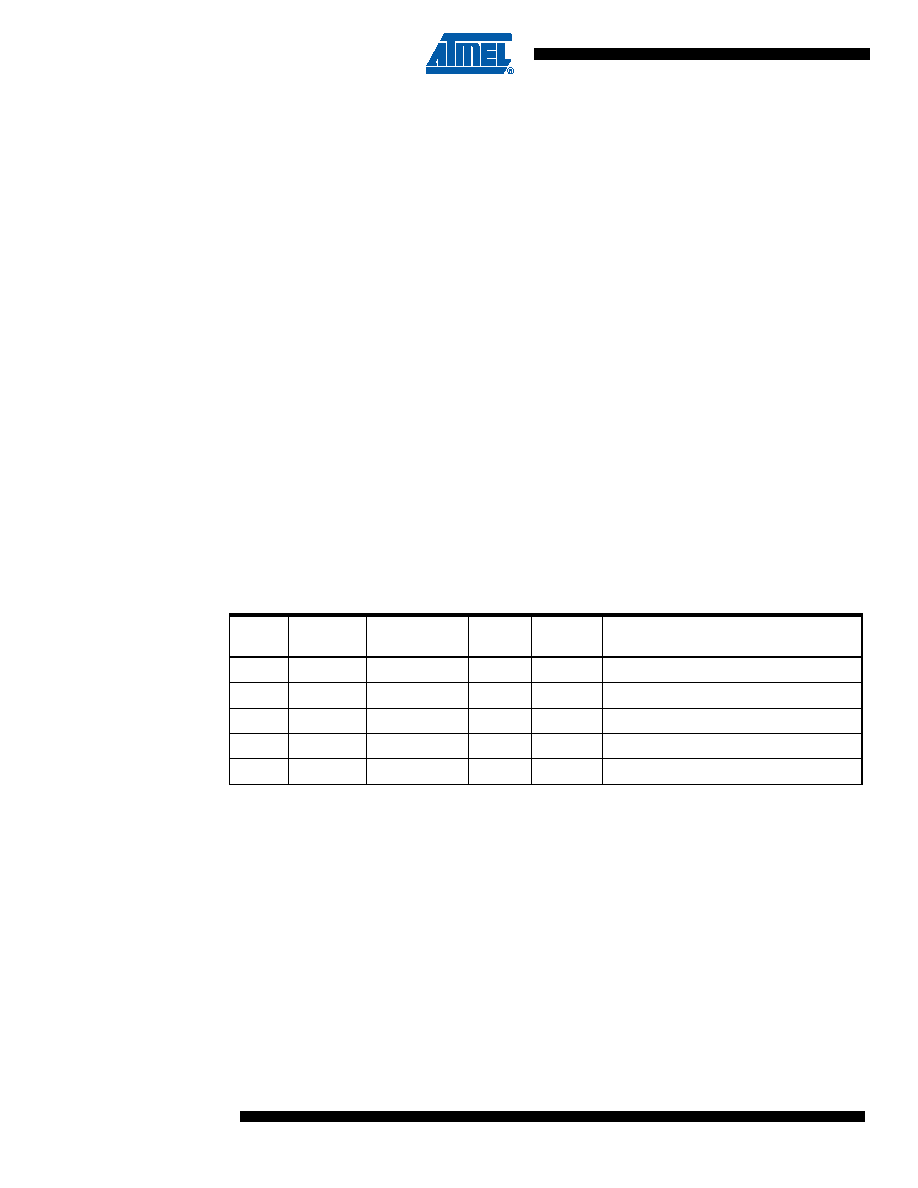
Table 10-1 summarizes the control signals for the pin value.
10.2.4
Reading the Pin Value
Independent of the setting of Data Direction bit DDxn, the port pin can be read through the
PINxn Register bit. As shown in Figure 10-2 on page 49, the PINxn Register bit and the preced-
ing latch constitute a synchronizer. This is needed to avoid metastability if the physical pin
changes value near the edge of the internal clock, but it also introduces a delay. Figure 10-3 on
page 51 shows a timing diagram of the synchronization when reading an externally applied pin
value. The maximum and minimum propagation delays are denoted tpd,max and tpd,min
respectively.
Table 10-1.
Port Pin Configurations
DDxn
PORTxn
PUD
(in MCUCR)
I/O
Pull-up
Comment
0
X
Input
No
Tri-state (Hi-Z)
0
1
0
Input
Yes
Pxn will source current if ext. pulled low.
0
1
Input
No
Tri-state (Hi-Z)
1
0
X
Output
No
Output Low (Sink)
1
X
Output
No
Output High (Source)
相关PDF资料 |
PDF描述 |
|---|---|
| ATTINY15L-1SU | IC MCU AVR 1K FLASH 1.6MHZ 8SOIC |
| ATTINY2313-20SUR | IC MCU AVR 2K FLASH 20SOIC |
| ATTINY2313A-MMHR | IC MCU AVR 2K FLASH 3X3 20QFN |
| ATTINY26-16MQR | IC MCU AVR 2K 16MHZ IND 32QFN |
| ATTINY26L-8PU | IC MCU AVR 2K 5V 8MHZ 20-DIP |
相关代理商/技术参数 |
参数描述 |
|---|---|
| ATTINY13V-W-11 | 功能描述:8位微控制器 -MCU Microcontroller RoHS:否 制造商:Silicon Labs 核心:8051 处理器系列:C8051F39x 数据总线宽度:8 bit 最大时钟频率:50 MHz 程序存储器大小:16 KB 数据 RAM 大小:1 KB 片上 ADC:Yes 工作电源电压:1.8 V to 3.6 V 工作温度范围:- 40 C to + 105 C 封装 / 箱体:QFN-20 安装风格:SMD/SMT |
| ATTINY13-W | 功能描述:8位微控制器 -MCU Microcontroller RoHS:否 制造商:Silicon Labs 核心:8051 处理器系列:C8051F39x 数据总线宽度:8 bit 最大时钟频率:50 MHz 程序存储器大小:16 KB 数据 RAM 大小:1 KB 片上 ADC:Yes 工作电源电压:1.8 V to 3.6 V 工作温度范围:- 40 C to + 105 C 封装 / 箱体:QFN-20 安装风格:SMD/SMT |
| ATTINY13-W-11 | 功能描述:8位微控制器 -MCU Microcontroller RoHS:否 制造商:Silicon Labs 核心:8051 处理器系列:C8051F39x 数据总线宽度:8 bit 最大时钟频率:50 MHz 程序存储器大小:16 KB 数据 RAM 大小:1 KB 片上 ADC:Yes 工作电源电压:1.8 V to 3.6 V 工作温度范围:- 40 C to + 105 C 封装 / 箱体:QFN-20 安装风格:SMD/SMT |
| ATTINY15 | 制造商:ATMEL 制造商全称:ATMEL Corporation 功能描述:8-BIT AVR㈢ Microcontroller with 1K Byte Flash |
| ATTINY15(PDIP) | 制造商:未知厂家 制造商全称:未知厂家 功能描述:Microcontroller |
发布紧急采购,3分钟左右您将得到回复。