- 您现在的位置:买卖IC网 > Datasheet目录396 > BBA-519-A (Linx Technologies Inc)MODULE RF AMP HI-POWER BROADBAND Datasheet资料下载
参数资料
| 型号: | BBA-519-A |
| 厂商: | Linx Technologies Inc |
| 文件页数: | 5/7页 |
| 文件大小: | 0K |
| 描述: | MODULE RF AMP HI-POWER BROADBAND |
| 产品目录绘图: | BBA-519-A Top BBA-519-A Side |
| 标准包装: | 50 |
| 频率: | 10MHz ~ 3GHz |
| P1dB: | 18.5dBm(70.8mW) |
| 增益: | 18dB |
| 噪音数据: | 4.8dB |
| RF 型: | 通用 |
| 电源电压: | 5V |
| 电流 - 电源: | 35mA ~ 60mA |
| 测试频率: | 1GHz |
| 封装/外壳: | 模块 |
| 包装: | 管件 |
�� �
�
�BOARD� LAYOUT� GUIDELINES�
�If� you� are� at� all� familiar� with� RF� devices,� you� may� be� concerned� about�
�specialized� board� layout� requirements.� Fortunately,� because� of� the� care� taken� by�
�Linx� in� designing� the� modules,� integrating� them� is� very� straightforward.� Despite�
�this� ease� of� application,� it� is� still� necessary� to� maintain� respect� for� the� RF� stage�
�and� exercise� appropriate� care� in� layout� and� application� in� order� to� maximize�
�performance� and� ensure� reliable� operation.� The� antenna� can� also� be� influenced�
�by� layout� choices.� Please� review� this� data� guide� in� its� entirety� prior� to� beginning�
�your� design.� By� adhering� to� good� layout� principles� and� observing� some� basic�
�design� rules,� you� will� be� on� the� path� to� RF� success.�
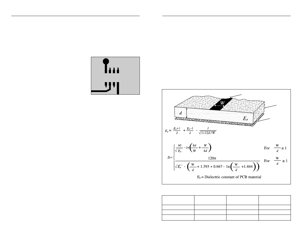
�MICROSTRIP� DETAILS�
�A� transmission� line� is� a� medium� whereby� RF� energy� is� transferred� from� one�
�place� to� another� with� minimal� loss.� This� is� a� critical� factor,� especially� in� high-�
�frequency� products� like� Linx� RF� modules,� because� the� trace� leading� to� the�
�module’s� antenna� can� effectively� contribute� to� the� length� of� the� antenna,�
�changing� its� resonant� bandwidth.� In� order� to� minimize� loss� and� detuning,� some�
�form� of� transmission� line� between� the� antenna� and� the� module� should� be� used,�
�unless� the� antenna� can� be� placed� very� close� (<1/8in.)� to� the� module.� One�
�common� form� of� transmission� line� is� a� coax� cable,� another� is� the� microstrip.� This�
�term� refers� to� a� PCB� trace� running� over� a� ground� plane� that� is� designed� to� serve�
�The� adjacent� figure� shows� the� suggested�
�PCB� footprint� for� the� module.� The� actual� pad�
�dimensions� are� shown� in� the� Pad� Layout�
�section� of� this� manual.� A� ground� plane� (as�
�large� as� possible)� should� be� placed� on� a�
�lower� layer� of� your� PC� board� opposite� the�
�module.� This� ground� plane� can� also� be� critical�
�to� the� performance� of� your� antenna,� which� will�
�be� discussed� later.� There� should� not� be� any�
�ground� or� traces� under� the� module� on� the�
�same� layer� as� the� module,� just� bare� PCB.�
�GROUND� PLANE�
�ON� LOWER� LAYER�
�Figure� 7:� Suggested� PCB� Layout�
�as� a� transmission� line� between� the� module� and� the� antenna.� The� width� is� based�
�on� the� desired� characteristic� impedance� of� the� line,� the� thickness� of� the� PCB,�
�and� the� dielectric� constant� of� the� board� material.� For� standard� 0.062in� thick� FR-�
�4� board� material,� the� trace� width� would� be� 111� mils.� The� correct� trace� width� can�
�be� calculated� for� other� widths� and� materials� using� the� information� below.� Handy�
�software� for� calculating� microstrip� lines� is� also� available� on� the� Linx� website,�
�www.linxtechnologies.com.�
�Trace�
�During� prototyping,� the� module� should� be� soldered� to� a� properly� laid-out� circuit�
�board.� The� use� of� prototyping� or� “perf”� boards� will� result� in� horrible� performance�
�and� is� strongly� discouraged.�
�No� conductive� items� should� be� placed� within� 0.15in� of� the� module’s� top� or� sides.�
�Do� not� route� PCB� traces� directly� under� the� module.� The� underside� of� the� module�
�has� numerous� signal-bearing� traces� and� vias� that� could� short� or� couple� to� traces�
�on� the� product’s� circuit� board.�
�The� module’s� ground� lines� should� each� have� their� own� via� to� the� ground� plane�
�and� be� as� short� as� possible.�
�The� module� should,� as� much� as� reasonably� possible,� be� isolated� from� other�
�components� on� your� PCB,� especially� high-frequency� circuitry� such� as� crystal�
�oscillators,� switching� power� supplies,� and� high-speed� bus� lines.� Make� sure�
�internal� wiring� is� routed� away� from� the� module� and� antenna,� and� is� secured� to�
�prevent� displacement.�
�The� power� supply� filter� should� be� placed� close� to� the� module’s� V� CC� line.�
�In� some� instances,� a� designer� may� wish� to� encapsulate� or� “pot”� the� product.�
�Many� Linx� customers� have� done� this� successfully;� however,� there� are� a� wide�
�variety� of� potting� compounds� with� varying� dielectric� properties.� Since� such�
�compounds� can� considerably� impact� RF� performance,� it� is� the� responsibility� of�
�the� designer� to� carefully� evaluate� and� qualify� the� impact� and� suitability� of� such�
�Figure� 8:� Microstrip� Formulas�
�Board�
�Ground� plane�
�materials.�
�The� trace� from� the� module� to� the� antenna� should� be� kept� as� short� as� possible.�
�Dielectric� Constant� Width/Height� (W/d)�
�Effective� Dielectric�
�Constant�
�Characteristic�
�Impedance�
�A� simple� trace� is� suitable� for� runs� up� to� 1/8-inch� for� antennas� with� wide�
�bandwidth� characteristics.� For� longer� runs� or� to� avoid� detuning� narrow� bandwidth�
�antennas,� such� as� a� helical,� use� a� 50-ohm� coax� or� 50-ohm� microstrip�
�transmission� line� as� described� in� the� following� section.�
�4.80�
�4.00�
�2.55�
�1.8�
�2.0�
�3.0�
�3.59�
�3.07�
�2.12�
�50.0�
�51.0�
�48.0�
�Page� 8�
�Page� 9�
�相关PDF资料 |
PDF描述 |
|---|---|
| BBS3002-DL-E | MOSFET P-CH 60V 100A SMP-FD |
| BC6110A14-IQQA-R | BC6-HEADSET |
| BD1020HFV-TR | IC TEMP SENSOR ANLG OUT 5-HVSOF |
| BDE1204G-TR | IC TEMP SENSOR THERM 120C 5-SSOP |
| BDJ0851HFV-TR | IC TEMP SENSOR 85DEG C 5-HVSOF |
相关代理商/技术参数 |
参数描述 |
|---|---|
| BBA5500005 | 功能描述:155.52MHz LVPECL XO (Standard) Oscillator Surface Mount 3.3V Enable/Disable 制造商:txc corporation 系列:BB 包装:带卷(TR) 零件状态:有效 类型:XO(标准) 频率:155.52MHz 功能:启用/禁用 输出:LVPECL 电压 - 电源:3.3V 频率稳定度:±20ppm 工作温度:-20°C ~ 70°C 电流 - 电源(最大值):- 等级:- 安装类型:表面贴装 大小/尺寸:0.276" 长 x 0.197" 宽(7.00mm x 5.00mm) 高度:0.059"(1.50mm) 封装/外壳:6-SMD,无引线(DFN,LCC) 电流 - 电源(禁用)(最大值):* 标准包装:1,000 |
| BBA5600007 | 功能描述:156.25MHz LVPECL XO (Standard) Oscillator Surface Mount 3.3V Enable/Disable 制造商:txc corporation 系列:BB 包装:带卷(TR) 零件状态:有效 类型:XO(标准) 频率:156.25MHz 功能:启用/禁用 输出:LVPECL 电压 - 电源:3.3V 频率稳定度:±25ppm 工作温度:0°C ~ 70°C 电流 - 电源(最大值):- 等级:- 安装类型:表面贴装 大小/尺寸:0.276" 长 x 0.197" 宽(7.00mm x 5.00mm) 高度:0.059"(1.50mm) 封装/外壳:6-SMD,无引线(DFN,LCC) 电流 - 电源(禁用)(最大值):* 标准包装:1,000 |
| BBA5600014 | 功能描述:156.25MHz LVPECL XO (Standard) Oscillator Surface Mount 3.3V Enable/Disable 制造商:txc corporation 系列:BB 包装:带卷(TR) 零件状态:有效 类型:XO(标准) 频率:156.25MHz 功能:启用/禁用 输出:LVPECL 电压 - 电源:3.3V 频率稳定度:±50ppm 工作温度:-40°C ~ 85°C 电流 - 电源(最大值):- 等级:- 安装类型:表面贴装 大小/尺寸:0.276" 长 x 0.197" 宽(7.00mm x 5.00mm) 高度:0.059"(1.50mm) 封装/外壳:6-SMD,无引线(DFN,LCC) 电流 - 电源(禁用)(最大值):* 标准包装:1,000 |
| BBA5670003 | 功能描述:156.25MHz LVPECL XO (Standard) Oscillator Surface Mount 3.3V Enable/Disable 制造商:txc corporation 系列:BB 包装:带卷(TR) 零件状态:有效 类型:XO(标准) 频率:156.25MHz 功能:启用/禁用 输出:LVPECL 电压 - 电源:3.3V 频率稳定度:±50ppm 工作温度:-40°C ~ 85°C 电流 - 电源(最大值):- 等级:- 安装类型:表面贴装 大小/尺寸:0.276" 长 x 0.197" 宽(7.00mm x 5.00mm) 高度:0.059"(1.50mm) 封装/外壳:6-SMD,无引线(DFN,LCC) 电流 - 电源(禁用)(最大值):* 标准包装:1,000 |
| BBA6100004 | 功能描述:161.1328MHz LVPECL XO (Standard) Oscillator Surface Mount 3.3V Enable/Disable 制造商:txc corporation 系列:BB 包装:带卷(TR) 零件状态:有效 类型:XO(标准) 频率:161.1328MHz 功能:启用/禁用 输出:LVPECL 电压 - 电源:3.3V 频率稳定度:±50ppm 工作温度:0°C ~ 70°C 电流 - 电源(最大值):- 等级:- 安装类型:表面贴装 大小/尺寸:0.276" 长 x 0.197" 宽(7.00mm x 5.00mm) 高度:0.059"(1.50mm) 封装/外壳:6-SMD,无引线(DFN,LCC) 电流 - 电源(禁用)(最大值):* 标准包装:1,000 |
发布紧急采购,3分钟左右您将得到回复。